


What are the meaning of Vdd and Vss? Vcc and Vee?? GND? - Mis Circuitos
It has always been a bit intriguing and even confusing the nomenclature of these power voltages (Vdd and Vss) or (Vcc and Vee).
The following pictures are worth a thousand words…

VDD, VSS, Vcc and Vee in Cadence
schematic
Nowadays it is always used Vdd and Vss to refer to the positive and negative voltage respectively. Vdd normally was used to be 5V but nowadays is 3.3V or even lower 1.8V or 1.2V. Vss is referred to be zero volts.
But I was taught, in the high school and during my first years of electronics, that Vcc is the positive voltage (usually 5 volts) but when we get to some circuits we find pins Vdd, Vss and Vdd. Maybe many have not been intrigued by this but if you are reading this probably yes. So let’s continue:
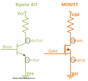
What is the nomenclature?
This depends on the type of transistors that the electronic device has internally the microchip, circuit or microcontroller.
If internally formed by bipolar transistors (BJT), then the nomenclature is:
–Vcc for being the voltage applied to the Collector of the transistors
–Vee for being the voltage applied to the transistor Emitter leg
If internally built by Field Effect Transistors (FET, MOSFET), the nomenclature is:
–Vss for being the voltage applied to the transistor Source pin
–Vdd for being the voltage applied to the Drain of the transistors
So what is the polarity of each one?
Because NPN and NMOS transistors are used as a reference:


 5116
5116


 被折叠的 条评论
为什么被折叠?
被折叠的 条评论
为什么被折叠?
 到【灌水乐园】发言


