


特性
• 宽输入电压:4V~24V,耐压 30V
• 集成低 Rdson MOS,效率高达 97%
• 充电管理(短路充电、恒流充电、恒压充电、自动复充)
• 可调节的输入电流限制和充电电流,电流最大4A
• 可配置的电池电压,适用于 1-4 节锂电池
• 可调节的充电安全定时器
• NTC 支持 JEITA 电池温度保护标准
• 可持续监控 IC 温度,过温时自动降低充电电流,确保 IC 在正常温度范围内工作
• 充电状态指示
• 可调输入过压和欠压保护
• 电池过压保护
• 集成外部 NMOS隔离驱动和 PMOS路径管理驱动,支持充电和系统电源的路径管理
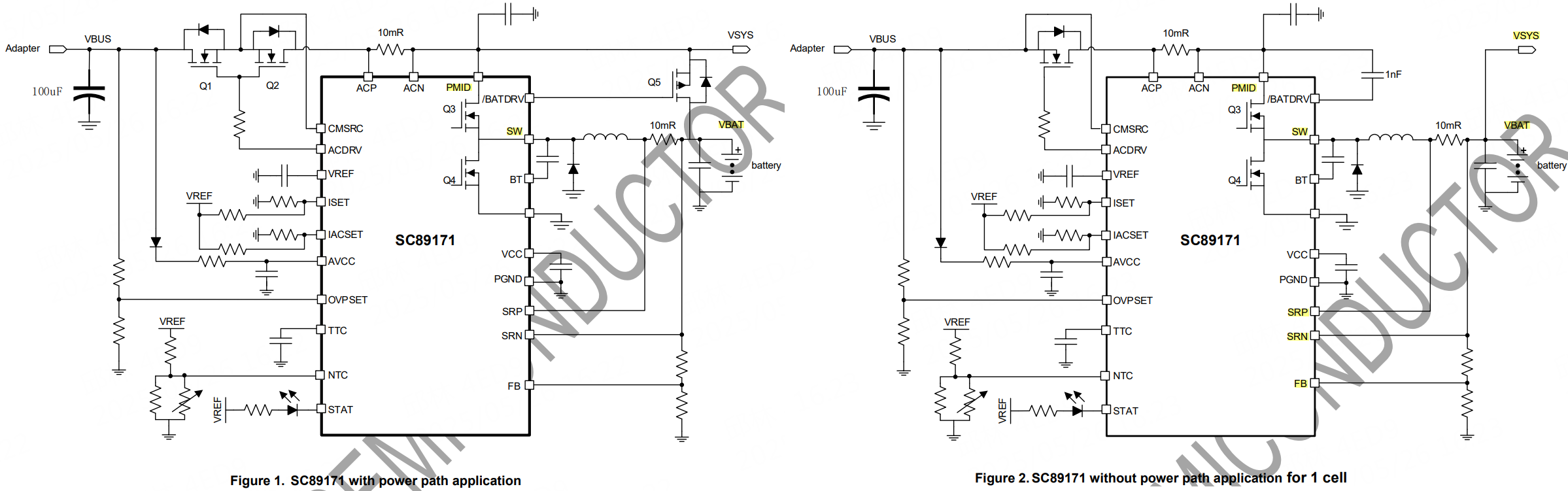
应用电路
引脚
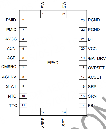
| 引脚 | 名字 | I/O | 描述 |
|---|---|---|---|
| 1, 24 | SW | I/O | 连接外部电感 |
| 2, 3 | PMID | I | 内部降压buck电压输入。连接到反向阻断MOSFET的漏极。 |
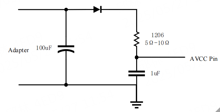
| 4 | AVCC | I | 芯片供电。放置1µF电容在AVCC 和 AGND,且尽量靠近芯片 |
| 5 | ACN | I | 适配器输入电流采样负输入 |
| 6 | ACP | I | 适配器输入电流采样正输入 |
| 7 | CMSRC | O | Connect to common source of ACFET and reverse blocking FET. |
| 8 | ACDRV | O | Blocking FET driver output. Connect to the gate of blocking FET. |
| 9 | STAT | O | Charge status indication. Open drain output. Connect it to pull-up, |
| 10 | NTC | I | 温度感应引脚。连接到电池单元内部的负温度系数 (NTC) 热敏电阻,以感应电池单元温度以进行保护。将此引脚短接到地以禁用此功能。 |
| 11 | TTC | I | 安全定时器和终止控制。低:禁用安全定时器和充电终止 高:仅禁用安全定时器 |
| 12 | VREF | O | 3.3V参考电压输出,放置1µF电容在VREF 和 AGND,且尽量靠近芯片 |
| 13 | ISET | I | 充电电流设置引脚 |
| 14 | FB | I | 电池充电电压反馈引脚,内部参考为 2.1V。 |
| 15 | SRN | I | 充电电流采样负输入 |
| 16 | SRP | I | 充电电流采样正输入 |
| 17 | IACSET | I | 适配器输入电流限制设置引脚 |
| 18 | OVPSET | I | 适配器输入电压设置引脚。连接从 VBUS 到 AGND 的电阻分压器以设置充电器工作范围。 |
| 19 | /BATDRV | O | BATFET 栅极驱动器输出。 |
| 20 | VCC | O | 内部 LDO 输出。连接一个1uF 电容器。 |
| 21 | BT | O | Bootstrap 引脚。在 BT 引脚和 SW 引脚之间连接一个 100nF 的陶瓷电容器,为内部驱动器电路提供偏置电压。 |
| 22, 23 | PGND | O | power ground. |
| 25 | AGND | I/O | Exposed thermal pad. Connected with power ground through vias. |
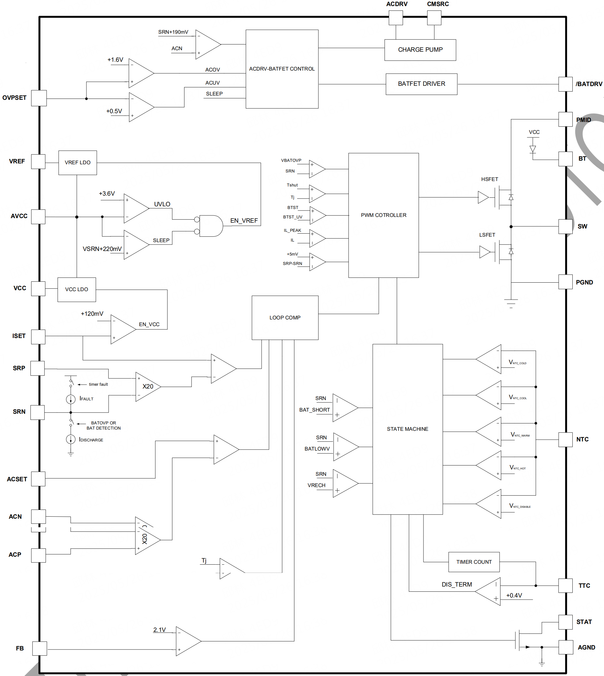
框图
描述
芯片上电
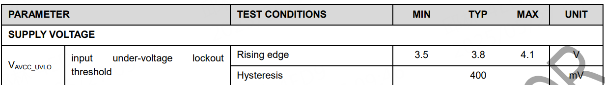
当AVCC电压大于VUVLO,芯片就上电。芯片退出休眠模式后就开始充电周期。
休眠模式
当AVCC电压大于VUVLO,但是AVCC<VSRN+160mV,芯片进入休眠模式。在休眠模式,VREF输出关闭,充电禁止,STAT引脚变成高阻态。
VREF LDO
芯片内部集成输出VREF电压的LDO,用于适配器输入电流设置、充电电流设置电路。当AVCC电压大于VUVLO,且不处于休眠模式,LDO就工作。
VCC LDO
芯片内部集成输出VCC 5V电压的LDO,用于MOS管驱动。当VISET>120mV且AVCC上电,LDO开始工作。
当VISET<120mV,芯片进入待机模式,VCC LDO禁止,充电禁止。
电源路径管理
负载供电可以从适配器或电池自动切换。当处于休眠模式,只有电池存在时,BATFET会打开,让电池给负载供电。
当插入适配器,芯片退出休眠模式,BATFET关闭,ACFET打开,让适配器给负载供电。
当适配器拔出或插入了过压的适配器,ACFET关闭,然后BATFET打开,让电池给负载供电。
充电管理
充电曲线如下:
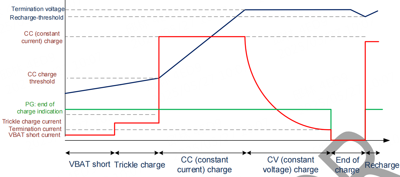
当下面条件都满足开始充电:
- VISET>120mV
- 不在欠压模式(VAVCC> VUVLO)
- 不在休眠模式(VAVCC > VSRN)
- 不在n ACOV 或 ACUV模式(0.5 V< VOVPSET <1.6 V)
- 上电后会延时1.5s才开始充电
- VREF和VCC的LDO电压正常
- 热关断无效
- 无NTC故障
- ACFET打开
- 没有安全定时器触发
电池检测
当AVCC上电或VBAT跌落到小于VBAT_RECH(battery recharge voltage),芯片启动电池检测流程。
Step1: POR and VBAT < recharge voltage is triggered.
Step2: 8mA discharge current from SRN to GND and 1s timer starts. If VBAT > V BAT_TRK and 1s timer expires, battery is present and IC start charging. Otherwise battery is absent, then go to next step.
Step3: 125mA charging current to VBAT and 500ms timer starts. If VBAT < V BAT_RECH and lasting for 500ms, battery is present and IC start charging. Otherwise battery is absent, STAT pin is blinking, then repeat the battery detection cycle.


涓流充电
当VBAT小于VBAT_TRK (trickle charge threshold),芯片进行涓流充电。涓流充电时的充电电流为ISET引脚设置电流的十分之一。
涓流充电电流最小值为120mA。

恒流充电
当VBAT电压大于VBAT_TRK,芯片进入恒流充电模式。
恒流充电电流设置:
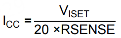
当VISET小于40mV,芯片禁止。当VISET大于120mV,芯片使能。ISET可以用作芯片使能脚。
恒电压充电
当VBAT电压超过98%的VBAT_TRGT电压后,芯片进入恒电压充电。
电池的电压可以设置:
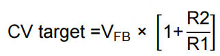
VFB=2.1V。
因此单节电池,取R1=100K、R2=100K
充电结束 end of charge (EOC)
当满足下面调节,芯片认为充电完成:
- 终止电压:VBAT电压超过98%的VBAT_TRGT
- 终止电流:充电电流小于终止电流。终止电流公式:
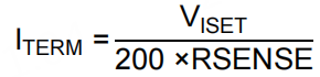
- 上述两个条件满足后稳定了500ms。
当充电完成,STAT输出高阻。
EOC is disabled when IC is in IINDPM or thermal regulation.
In EOC phase, the IC stops charging, ACFET is still turned on to provide power from adapter to system.
重新开始充电
当VBAT小于VVBAT_RECH,芯片重新开始充电。
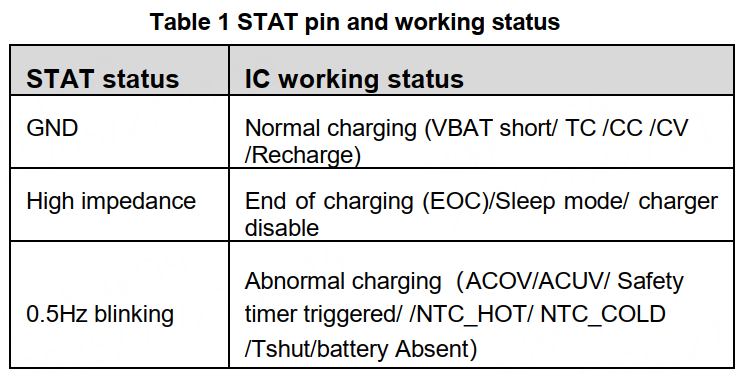
充电状态指示
当处于涓流/恒流/恒压充电模式,STAT输出地。当充电完成,STAT输出高阻。
当发生故障,STAT在地和高阻间以0.5Hz频率切换。
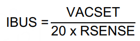
适配器输入电流限制
公式:
NTC
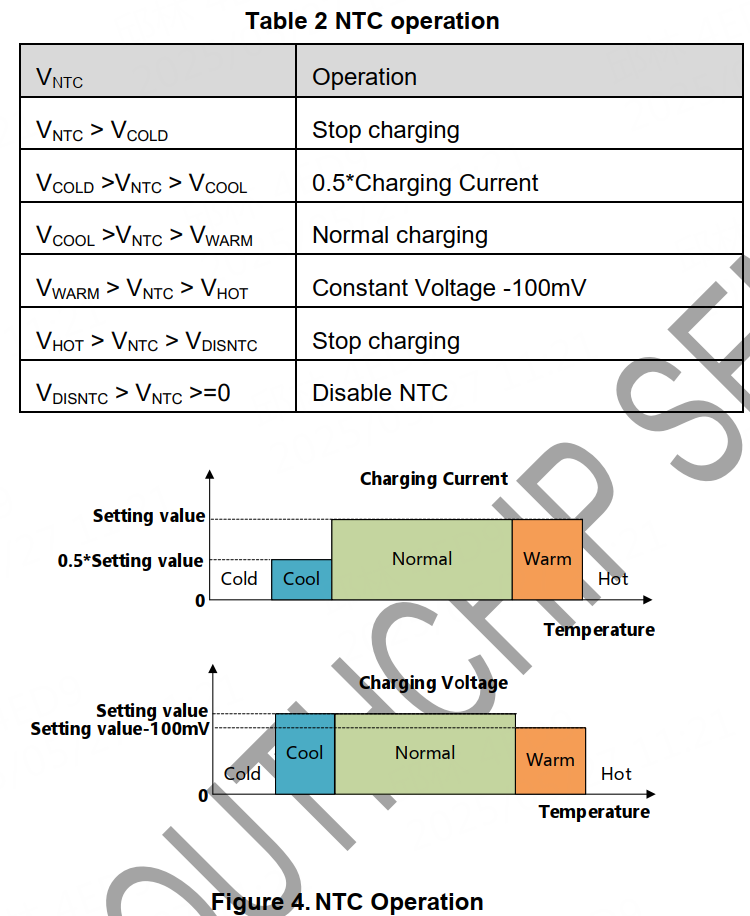
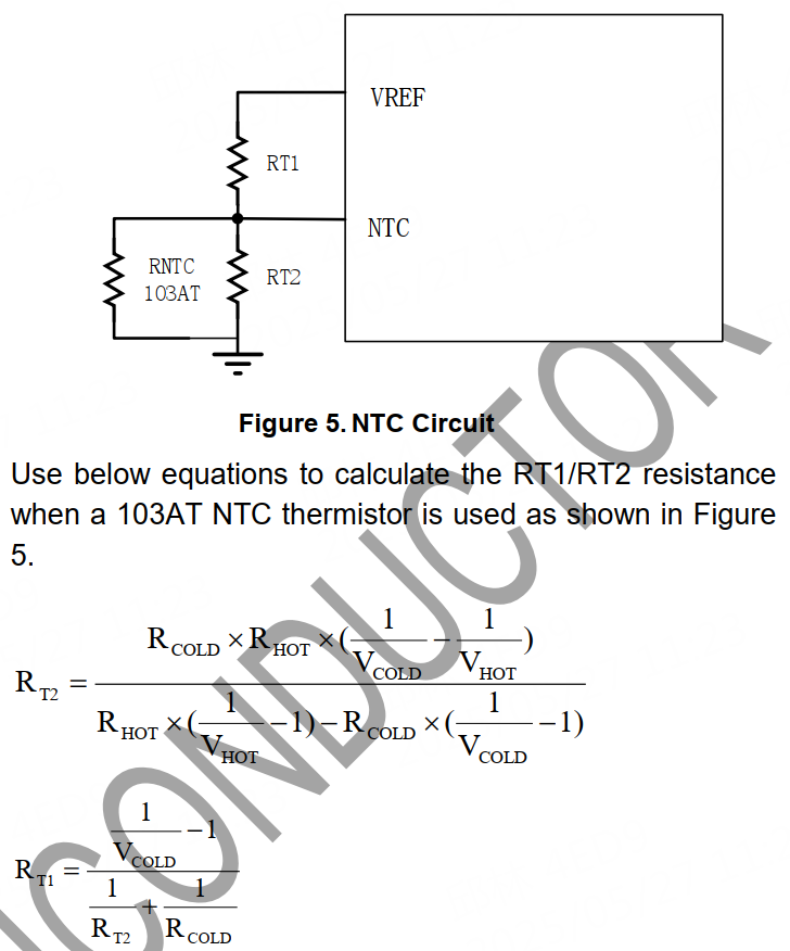
Where, RHOT is the NTC resistance at the hot temperature
threshold, RCOLD is the resistance at the cold threshold.
For example, set 0 °C(cold) to 60 °C (hot) to be the
charging range. So RCOLD = 28.71 KΩ, RHOT =2.99 KΩ
(resistance of 103AT thermistor at 0°C and 60°C)
So the calculation results are:
RT1=2.22 KΩ, RT2=6.64 KΩ;
With above setting, the cool temperature and warm
temperature are 10 °C and 45 °C.
输入欠压、过压保护
当OVPSET引脚电压大于1.6V或小于0.5V,芯片进入过压、欠压保护。芯片停止buck、ACFET关闭、BATFET打开,STAT闪烁报警。
VBAT过压保护
当芯片检测到VBAT电压大于104%设置的电池电压,芯片停止buck,启动6mA放电电流从SRP/SRN 到 AGND。高侧MOS不会打开直到电池电压低于102%。
电池过压状态持续了超过30ms,充电禁止。
VBAT短路保护
当芯片检测到VBAT电压小于VBAT_SHORT,会触发VBAT短路保护,芯片限制短路电流为100mA。
充电过流保护
芯片逐周期检测电感峰值电流,会把峰值电流钳位在9A。
充电欠电流保护
When SRP-SRN voltage decreases below 5mV, the lowside FET is turned off for the rest of the switching cycle. IC
Working in DCM mode. During discontinuous conduction
mode, the low-side FET turns on for a short period of time
when the bootstrap capacitor voltage drops below 4 V to
provide refresh charge for the capacitor.
安全定时器
芯片具有内部定时器来避免超时充电。涓流充电阶段时间限时为30分钟,当芯片进入恒流阶段,限时时间由TTC引脚和AGND间的电容来设置,公式为:
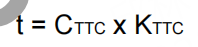
KTTC = 6min/nF for fast charge phase (including CC and CV phase), 0.3min/nF for trickle charge phase.
比如当CTTC= 100nF,则恒流阶段限时时间=100x6=600分钟。
TTC引脚同时可以用作安全定时器和终止控制。接AGND:禁用安全定时器和充电终止 接VREF:仅禁用安全定时器
当安全定时器超时但充电未完成,芯片会进入关断模式,STAT闪烁报警。芯片根据电池电压提供两种恢复方式:
Condition 1: VBAT > VBAT_RECH and safety timer is triggered.
Recovery Method: VBAT< VBAT_RECH will clear the timer fault
and battery detection will begin. A POR or taking ISET pin
below 40 mV will also clear the fault.
Condition 2: VBAT < VBAT_RECH and safety timer is triggered.
2mA charging current is used to detect a battery removal
condition and remains on as long as the battery voltage
stays below the recharge threshold. If battery is removed,
VBAT> VBAT_RECH, 2mA charging current is disabled, and
executes the recovery method in condition 1.
Thermal Regulation and Shutdown
In charging process, SC89171 keeps monitoring junction
temperature. When IC detects Tj >120°C, it enters into
thermal regulation loop and charging current is decreased
gradually. If Tj still exceeds 120°C, charging current can be
decreased to 0.
Once the SC89171 detects the junction temperature rises
above 150°C, it shuts down the whole chip. When the
temperature falls below 130°C, the chip is enabled again.
应用
输入滤波电路设计
当适配器热插入,寄生电感和电容会产生电压尖峰,输入电路需要根据应用来设计防止AVCC引脚发生过压故障。
输入输出电容
Since MLCC ceramic capacitor has good high frequency filtering
and low ESR, X5R or X7R capacitors are recommended for
input capacitors. Three 10uF input capacitors in PMID is
enough for most applications.
X5R or X7R MLCC capacitors are
recommended for output capacitors. 2x10uF output
capacitors is enough for most applications.
电感
2.2μH ~ 3.3 μH inductor is recommended for loop stability.


 1410
1410

 被折叠的 条评论
为什么被折叠?
被折叠的 条评论
为什么被折叠?
 到【灌水乐园】发言


