


一、基本介绍(8核 A55)
全志科技T527采用多核异构设计,集成了CPU、GPU、NPU、DSP、MCU等各种计算单元,为各种复杂场景的多任务处理、专用数据处理以及算法应用提供了高效且灵活的解决方案。
其中:
· T527集成了8核1.8GHz ARM CortexTM-A55内核,能够高效处理系统调度和并发业务,确保产品更好的性能表现和交互体验;
· G57 GPU则为游戏体验、多屏显示及多屏互动提供了图形应用支撑;
· 独立的NPU,算力高达2Tops,为端侧语音及自然语言处理,图像处理及画质增强等AI应用提供了性能支持;
· 专用DSP能够广泛应用于图像、音频及数字信号处理的专用领域,为影音娱乐、工业生产提供了专属算力;
· RISC-V内核运行RTOS系统,为工业及机器人系统上的实时处理、高速响应以及工业级的稳定运行提供了重要保障。
二、DTS信息
cpus {
        #address-cells = <2>;
        #size-cells = <0>;

        cpu0: cpu@0 {
            device_type = "cpu";
            compatible = "arm,cortex-a55";
            reg = <0x0 0x0>;
            enable-method = "psci";
            cpu-idle-states = <&CPU_SLEEP_0 &CLUSTER_SLEEP_0>;
            capacity-dmips-mhz = <922>;
            clocks = <&cpupll_ccu CLK_PLL_CPU1>;
            operating-points-v2 = <&cluster0_opp_table>;
            #cooling-cells = <2>;
            dynamic-power-coefficient = <286>;
        };

        cpu1: cpu@100 {
            device_type = "cpu";
            compatible = "arm,cortex-a55";
            reg = <0x0 0x100>;
            enable-method = "psci";
            cpu-idle-states = <&CPU_SLEEP_0 &CLUSTER_SLEEP_0>;
            capacity-dmips-mhz = <922>;
            clocks = <&cpupll_ccu CLK_PLL_CPU1>;
            operating-points-v2 = <&cluster0_opp_table>;
            #cooling-cells = <2>;
        };

        cpu2: cpu@200 {
            device_type = "cpu";
            compatible = "arm,cortex-a55";
            reg = <0x0 0x200>;
            enable-method = "psci";
            cpu-idle-states = <&CPU_SLEEP_0 &CLUSTER_SLEEP_0>;
            capacity-dmips-mhz = <922>;
            clocks = <&cpupll_ccu CLK_PLL_CPU1>;
            operating-points-v2 = <&cluster0_opp_table>;
            #cooling-cells = <2>;
        };

        cpu3: cpu@300 {
            device_type = "cpu";
            compatible = "arm,cortex-a55";
            reg = <0x0 0x300>;
            enable-method = "psci";
            cpu-idle-states = <&CPU_SLEEP_0 &CLUSTER_SLEEP_0>;
            capacity-dmips-mhz = <922>;
            clocks = <&cpupll_ccu CLK_PLL_CPU1>;
            operating-points-v2 = <&cluster0_opp_table>;
            #cooling-cells = <2>;
        };

        cpu4: cpu@400 {
            device_type = "cpu";
            compatible = "arm,cortex-a55";
            reg = <0x0 0x400>;
            enable-method = "psci";
            cpu-idle-states = <&CPU_SLEEP_0 &CLUSTER_SLEEP_0>;
            capacity-dmips-mhz = <1024>;
            clocks = <&cpupll_ccu CLK_PLL_CPU3>;
            operating-points-v2 = <&cluster1_opp_table>;
            #cooling-cells = <2>;
            dynamic-power-coefficient = <354>;
        };

        cpu5: cpu@500 {
            device_type = "cpu";
            compatible = "arm,cortex-a55";
            reg = <0x0 0x500>;
            enable-method = "psci";
            cpu-idle-states = <&CPU_SLEEP_0 &CLUSTER_SLEEP_0>;
            capacity-dmips-mhz = <1024>;
            clocks = <&cpupll_ccu CLK_PLL_CPU3>;
            operating-points-v2 = <&cluster1_opp_table>;
            #cooling-cells = <2>;
        };

        cpu6: cpu@600 {
            device_type = "cpu";
            compatible = "arm,cortex-a55";
            reg = <0x0 0x600>;
            enable-method = "psci";
            cpu-idle-states = <&CPU_SLEEP_0 &CLUSTER_SLEEP_0>;
            capacity-dmips-mhz = <1024>;
            clocks = <&cpupll_ccu CLK_PLL_CPU3>;
            operating-points-v2 = <&cluster1_opp_table>;
            #cooling-cells = <2>;
        };

        cpu7: cpu@700 {
            device_type = "cpu";
            compatible = "arm,cortex-a55";
            reg = <0x0 0x700>;
            enable-method = "psci";
            cpu-idle-states = <&CPU_SLEEP_0 &CLUSTER_SLEEP_0>;
            capacity-dmips-mhz = <1024>;
            clocks = <&cpupll_ccu CLK_PLL_CPU3>;
            operating-points-v2 = <&cluster1_opp_table>;
            #cooling-cells = <2>;
        };
三、测试方法
1.stress-ng CPU压力测试
(1)基本 CPU 压力测试
stress-ng --cpu 4 --timeout 60s
测试结果:

(2)浮点运算压力测试
stress-ng --cpu 4 --cpu-method flops --timeout 60s
(3)矩阵乘法压力测试
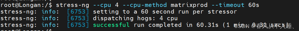
stress-ng --cpu 4 --cpu-method matrixprod --timeout 60s
测试结果:
(4)质数计算压力测试
stress-ng --cpu 4 --cpu-method prime --timeout 60s
测试结果:

(5)混合 CPU 压力测试
stress-ng --cpu 4 --cpu-method mix --timeout 60s
(6)多线程 CPU 压力测试(75% 负载)
stress-ng --cpu 4 --cpu-load 75 --timeout 60s
测试结果:

(7)同时对 CPU 和内存进行压力测试
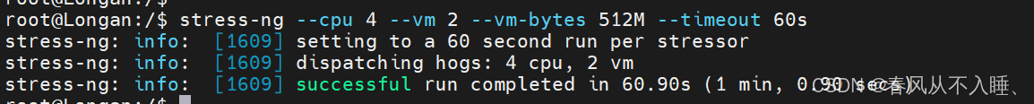
stress-ng --cpu 4 --vm 2 --vm-bytes 512M --timeout 60s
测试结果:
stress-ng --cpu 8 --cpu-load 70 --vm 2 --vm-bytes 512M --timeout 60s
测试结果:

taskset -c 1 stress-ng --cpu 1 --vm 1 --vm-bytes 512M --timeout 60s
测试结果:

(8)同时8核 CPU MEM压力测试
#taskset 指定核
taskset -c 0 stress-ng --cpu 1 --vm 1 --vm-bytes 400M --timeout 60s &
taskset -c 1 stress-ng --cpu 1 --vm 1 --vm-bytes 400M --timeout 60s &
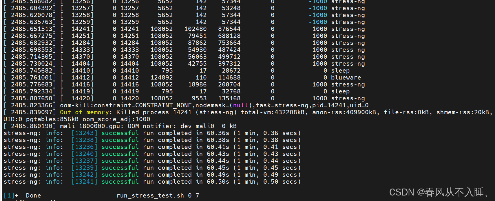
(9)8核
run_stress_test.sh 0 7 &
#!/bin/bash

# 检查参数是否正确
if [ "$#" -ne 2 ]; then
    echo "Usage: $0 <start_core> <end_core>"
    exit 1
fi

# 获取输入参数
start_core=$1
end_core=$2

# 检查 start_core 和 end_core 是否合法
if [ "$start_core" -gt "$end_core" ] || [ "$end_core" -gt 7 ]; then
    echo "Invalid core range: $start_core-$end_core"
    exit 1
fi

# 循环遍历指定的核心范围,运行压力测试
for ((core=start_core; core<=end_core; core++)); do
    echo "Running stress test on CPU core $core..."
    taskset -c $core stress-ng --cpu 1 --vm 1 --vm-bytes 512M --timeout 60s
done

echo "Stress test completed."
测试结果:


 1991
1991

 被折叠的 条评论
为什么被折叠?
被折叠的 条评论
为什么被折叠?
 到【灌水乐园】发言


