outstanding and out-of-order


Ordering model

AXI的控制和数据通道分离,可以带来很多好处。地址和控制信息相对数据的相位独立,可以先发地址,然后再是数据,这样自然而然的支持显著操作,也就是 outstanding 操作。Master访问slave的时候,可以不等需要的操作完成,就发出下一个操作。这样,可以让slave在控制流的处理上流水起来,达到提速的作 用。同时对于master,也许需要对不同的地址和slave就行访问,所以可以对不同的slave 连续操作。而这样的操作,由于slave 返回数据的先后可能不按照master 发出控制的先后进行,导致出现了乱序操作(out of order )。

先看下ordering model​的几个概念:​

Outstanding

: The ability to issue multiple outstanding addresses means that masters can issue transaction addresses without waiting for earlier transactions to complete. This featurecan improve system performance because it enables parallel processing of transactions.


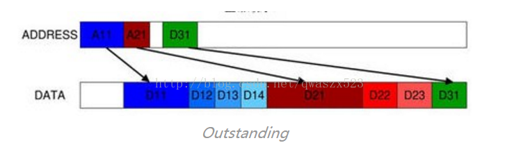
​​发出A11的addr后,在完成D11~D14的transfer之前,发出A21叫做outstanding。

Out-of-order : The ability to complete transactions out of order means that transactions to faster memory regions can complete without waiting for earlier transactions to slower memory regions. This feature can also improve system performance because it reducesthe effect of transaction latency.

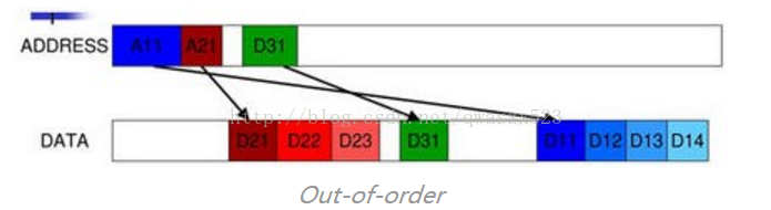
地址的顺序是A11,A21,A31,而数据顺序则可能是D2?,D3?,D1?,这个过程叫做Out-of-order

Interleaving:  Write data interleaving enables a slave interface to accept interleaved write data withdifferent AWID values. The slave declares a write data interleaving depth that indicatesif the interface can accept interleaved write data from sources with different AWIDvalues.

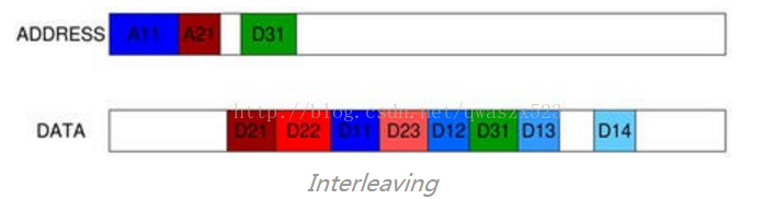
​D11和D12之间插入D23,叫做interleaving。

简单而言,outsatanding是对地址而言,一次burst还没结束,就可以发送下一相地址。而out-of-order和interleaving则是相对于 transaction,out-of-order说的是发送transaction​和接收的cmd之间的顺序没有关系,如先接到A的cmd,再接到B的cmd,则可以先发B的data,再发A的data;interleaving指的是A的data和B的data可以交错,如A1 B1 A2 B2 B3……

举个例子,从master和slave两个角色分别来看:

对于AXI master,先看写操作。如果分别发出WCMD1和WCMD2两个写命令给两个不同的slave,假设这两个写命令都是四拍的数据分别记为WDATA1_0,WDATA1_1,WDATA1_2,WDATA1_3,以及WDATA2_0,WDATA2_1,WDATA2_2,WDATA2_3。如果master在自己的写数据总线上,依次发出WDATA2_0,WDATA2_1,WDATA2_2,WDATA2_3,WDATA1_0,WDATA1_1,WDATA1_2,WDATA1_3,这就叫写out of order;如果master在自己的写数据总线上,依次发出WDATA2_0,WDATA1_0,WDATA2_1,WDATA1_1,WDATA2_2,WDATA2_3,WDATA1_2,WDATA1_3,这就叫写out of order且interleave;注意,不论是out of order还是interleave,同一个命令对应的四拍数据在内部必须是顺序的,不能乱序。比如,不允许出现WDATA2_1,WDATA1_0,WDATA2_0,WDATA1_1,WDATA2_2,WDATA2_3,WDATA1_2,WDATA1_3这样的。显然,你自己设计master时,如果是写操作,你不会主动发出out of oder和interleave的操作,因为这个明显增加了复杂度且没带来master自己的效率提高。再看master读,同样发出RCMD1和RCMD2两个读命令给不同的slave,由于不同slave的响应速度不同,就可能出现RCMD2对应的读数据先返回到master的情况;再考虑到复杂系统的总线设计,master依次接收到RDATA2_0,RDATA1_0,RDATA1_1,RDATA1_2,RDATA2_1,RDATA2_2,RDATA1_3,RDATA2_3这样的数据是有可能的,这就是读的out of order且interleave。所以,对于master,不建议发出out of order与interleave的写数据,但是必须支持out of order与interleave的读操作!同理,可以分析,对于slave,必须支持out of order与interleave的写操作,不建议返回out of order与interleave的读数据。在一个系统中,interleave会明显增加设计复杂度,其实可以约定master,slave以及连接总线都不要使用interleave,(另外可以配置depth ==1,达到不支持interleaving的目的)这样可以降低复杂度,但out of order是AXI特性,这个功能必须支持。

  • 24
    点赞
  • 114
    收藏
    觉得还不错? 一键收藏
  • 0
    评论
### 回答1: 设计sigma-delta转换器是一个复杂的过程,需要经过多个步骤。以下是在MATLAB / Simulink中设计sigma-delta转换器的一般过程: 1. 确定系统规格:首先,确定sigma-delta转换器的采样率、精度要求和输入输出范围等系统规格。 2. 模型建立:使用Simulink建立sigma-delta转换器的模型。该模型包括一个Σ(summing)节点、一个Δ(differential)节点和一个比较器节点。使用研究成果相关的数学模型,可以更准确地描述转换器的行为。 3. 参数选择:选择适当的参数来满足系统规格。包括选择合适的阶数和过采样率。过采样率越高,转换器的性能越好,但同时也会增加计算的复杂性和系统复杂度。 4. 仿真验证:使用Simulink对模型进行仿真验证。这可以帮助我们了解系统的性能如何受到不同参数选取的影响。 5. 优化调整:根据仿真结果,对转换器的参数和结构进行优化调整。例如,可以调整Σ节点和Δ节点之间的连接方式,或者优化误差补偿电路的设计。 6. 输出结果:根据优化后的模型,输出设计好的sigma-delta转换器的结果。这可以包括模型中各个节点和参数的数值值。 此外,在设计sigma-delta转换器的过程中,还需要考虑一些其他的因素,如抗噪声能力、计算要求、电路复杂度和成本等。根据具体的需求和约束条件,可以对上述过程进行调整和扩展,以获得最佳的设计结果。 总而言之,设计sigma-delta转换器需要经历模型建立、参数选择、仿真验证、优化调整和输出结果等多个步骤。通过这些步骤,可以获得一个满足系统要求的优化转换器设计。 ### 回答2: Sigma-delta (ΣΔ) converters are commonly used in analog-to-digital (ADC) and digital-to-analog (DAC) applications. They are known for their outstanding performance in terms of resolution, noise shaping, and dynamic range. To design a Sigma-delta converter in MATLAB/Simulink, we can follow the following steps: 1. Specify the converter's specifications: Determine the required resolution, sampling frequency, and input signal bandwidth to meet the desired performance requirements. 2. Model the Sigma-delta modulator: Create a Simulink model to represent the Sigma-delta modulator. This can be done by using Simulink blocks such as Adders, Delays, and Comparators. 3. Define the Analog-to-Digital Converter (ADC): Add the ADC block to the Simulink model and configure its parameters, such as the number of bits, input range, and sampling frequency. 4. Implement the digital decimation filter: Insert a digital decimation filter after the ADC block to remove out-of-band noise and further improve the overall performance. The decimation filter can be modeled using filter blocks in Simulink. 5. Evaluate the performance: Simulate the Simulink model with different input signals and study the system's response. Analyze the output waveform, signal-to-noise ratio (SNR), and other performance metrics to assess the design's effectiveness. 6. Optimize the design: Based on the performance analysis, make design adjustments to enhance the overall system's performance. This can involve modifying filter parameters, changing the modulator architecture, or adjusting the decimation filter design. 7. Verify the design: Validate the design by testing it with various input signals and comparing the simulation results with the desired specifications. 8. Implement the design: Once the design is finalized, the Sigma-delta converter can be implemented in hardware using appropriate components. In summary, to design a Sigma-delta converter in MATLAB/Simulink, we start by specifying the converter's specifications, modeling the modulator and ADC in Simulink, adding a digital decimation filter, evaluating the performance, optimizing the design, verifying the design, and finally implementing it in hardware.
评论
添加红包

请填写红包祝福语或标题

红包个数最小为10个

红包金额最低5元

当前余额3.43前往充值 >
需支付:10.00
成就一亿技术人!
领取后你会自动成为博主和红包主的粉丝 规则
hope_wisdom
发出的红包
实付
使用余额支付
点击重新获取
扫码支付
钱包余额 0

抵扣说明:

1.余额是钱包充值的虚拟货币,按照1:1的比例进行支付金额的抵扣。
2.余额无法直接购买下载,可以购买VIP、付费专栏及课程。

余额充值