


DDR系列文章分类地址:
(1)DDR3 基础知识分享
(2)DDR3 控制器 MIG IP 详解完整版 (AXI4&Vivado&Verilog)
(3)DDR3 控制器 MIG IP 详解完整版 (native&Vivado&Verilog)
(4)基于 DDR3 的串口传图帧缓存系统设计实现
(5)基于 DDR3 的native接口串口局部传图缓存系统设计实现
(6)基于 DDR3 的串口传图缓存系统设计实现
(7)基于 FPGA 的彩色图像灰度化的设计实现
文章目录
前言
结合串口接收模块和 tft 显示屏控制模块,设计一个基于 DDR3—Native接口的串口传图帧缓存系统。
提示:以下是本篇文章正文内容,下面案例可供参考
一、串口传图顶层系统设计框图
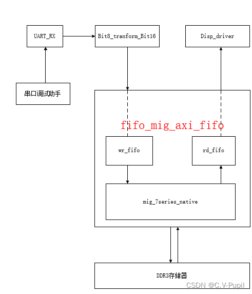
二、各模块说明
(1)uart_byte_rx 模块:负责串口图像数据的接收,该模块的设计前面章节已经有讲(可参考 串口接收)。
(2)bit8_trans_bit16 模块:将串口接收的每两个 8bit 数据转换成一个 16bit 数据(图像数据是 16bit 的 RGB565 的数据,电脑是通过串口将一个像素点数据分两次发送到 FPGA,FPGA 需将串口接收数据重组成 16bit 的图像数据),实现过程相对比较简单(可参考bit8_trans_bit16 模块)。
(3)disp_driver 模块:tft 屏显示驱动控制,对缓存在 DDR3 中的图像数据进行显示(可参考VGA成像原理)。
(4)wr_ddr3_fifo 模块:使用的 FIFO IP ,主要用于写入 DDR3 数据的缓存、解决数
据跨时钟域以及数据位宽的转换(IP生成参考 IP生成 )。
(5)rd_ddr3_fifo 模块:使用的 FIFO IP ,主要用于读出 DDR3 数据的缓存、解决数据
跨时钟域以及数据位宽的转换(IP生成参考 IP生成 )。
(6)fifo_ddr3_native_fifo 模块:主要是用于接口的转换,将 MIG IP 的Native接口换成与 FIFO
对接的接口(可参考第五节 )。
(7)mig_7series_native 模块: DDR3 控制器,使用的 Memory Interface Generator(MIG 7
Series)IP(可参考 DDR3 控制器 MIG IP 详解完整版 )。
(8)pll 模块:上述各个模块所需时钟的产生,使用 PLL IP。除去使用 IP 和前面章节讲过的模块外,还需要设计的模块包括 bit8_trans_bit16 模块和fifo_ddr3_native_fifo 模块(IP生成在下方有介绍)。
(9)顶层模块uart_ddr3_native_tft,用于实现上述模块的转换与连接(参考第三节)。
三、uart_ddr3_native_tft
该模块主要作用是串联其他模块,完成传图过程。其中个模块对应的介绍均在第二节后附有连接,以供参考。
`timescale 1ns / 1ns
//
// Create Date: 2023/06/20 08:58:45
// Module Name: uart_fifo_ddr3_fifo_tft

// Name: 小王在努力...
// Revision 0.01 - File Created
// Additional Comments:
//


module uart_ddr3_native_tft(
	  //System clock reset
	  input           clk50m        , //系统时钟输入,50MHz
	  input           reset_n       , //复位信号输入
	  //LED
	  output [3:0]    led           ,
	  //Uart interface
	  input           uart_rx       , //串口输入信号
	  //TFT Interface
	  output [15:0]   TFT_rgb       , //TFT数据输出
	  output          TFT_hs        , //TFT行同步信号
	  output          TFT_vs        , //TFT场同步信号
	  output          TFT_clk       , //TFT像素时钟
	  output          TFT_de        , //TFT数据使能
	  output          TFT_PWM       , //TFT背光控制
	  //DDR3 Interface
	  // Inouts
	  inout  [15:0]   ddr3_dq       ,
	  inout  [1:0]    ddr3_dqs_n    ,
	  inout  [1:0]    ddr3_dqs_p    ,
	  // Outputs
	  output [13:0]   ddr3_addr     ,
	  output [2:0]    ddr3_ba       ,
	  output          ddr3_ras_n    ,
	  output          ddr3_cas_n    ,
	  output          ddr3_we_n     ,
	  output          ddr3_reset_n  ,
	  output [0:0]    ddr3_ck_p     ,
	  output [0:0]    ddr3_ck_n     ,
	  output [0:0]    ddr3_cke      ,
	  output [0:0]    ddr3_cs_n     ,
	  output [1:0]    ddr3_dm       ,
	  output [0:0]    ddr3_odt
	);

     //pll interface
     wire loc_clk200M;
     wire loc_clk33M ;
	 wire loc_clk50M ;
     wire pll_locked ;


	 //bit8_trans_bit16 interface
	 wire [15:0]image_data;
	 wire image_data_valid;


	 // fifo_mig_axi_fifo Interface

	 wire [15:0]rdfifo_dout  ;
	 wire ui_clk             ;
	 wire ui_clk_sync_rst    ;

	 wire init_calib_complete;
	 wire rdfifo_rden        ;
	 wire rdfifo_wren;


	 //disp_driver interface
	 wire frame_begin;
     wire rdfifo_WR_EN;

    //--------------------------------------------------------
	//测试数据

    parameter test_count = 24'd32400,
	          test_count_div_8 = 24'd4050,
              uart_byte_cnt_x2  =  test_count*2;


   assign led = {
   init_calib_complete,pll_locked,rdfifo_WR_EN,TFT_vs};

	pll pll
  (
    // Clock out ports
    .clk_out1 (loc_clk50M   ), // output clk_out1
    .clk_out2 (loc_clk200M  ), // output clk_out2
    .clk_out3 (loc_clk33M   ), // output clk_out3
    .clk_out4 (loc_clk9m    ), // output clk_out4
    // Status and control signals
    .resetn   (reset_n      ), // input reset
    .locked   (pll_locked   ), // output locked
    // Clock in ports
    .clk_in1  (clk50m       )  // input clk_in1
  );


     //uart Interface
	 //------------------------------------------------------------------------


	 wire [7:0]uart_byte ;
	 wire uart_byte_vaild;


	uart_byte_rx#(
	   .CLK_FRQ(1000000000)
	  )
	  uart_byte_rx(
	   .clk      (loc_clk50M      ),
	   .reset_p  (ui_clk_sync_rst ),

	   .baud_set (3'd4            ), //115200bps
	   .uart_rx  (uart_rx         ),

	   .data_byte(uart_byte       ),
	   .rx_done  (uart_byte_vaild )  //一个字节数据有效的标志
	  );


	  //-----------------------------------------------------------------------------


	  //-----------------------------------------------------------------------------------------------

	  //-------------------------------
	  //    测试使用
	  //    测试时将124-142注释
	  //-------------------------------


	  // reg [23:0]uart_byte_cnt;
	  // reg [7:0]uart_byte ;
	  // reg uart_byte_vaild;

	  // always @ (posedge loc_clk50M or negedge ui_clk_sync_rst)
		// if(ui_clk_sync_rst)
		   // uart_byte_cnt <= 0;

		// else if (fifo_ddr3_native_fifo.wr_fifo_rst_busy == 1'b0)
			// begin
				// if (uart_byte_cnt == uart_byte_cnt_x2 )
			          // uart_byte_cnt <= uart_byte_cnt;

		        // else
			         // uart_byte_cnt <= uart_byte_cnt + 1;
		    // end
		// else
			// uart_byte_cnt <= 0;

	  // always @ (posedge loc_clk50M or negedge ui_clk_sync_rst)
		 // if(ui_clk_sync_rst)
			// uart_byte <= 0;
		// else if(fifo_ddr3_native_fifo.wr_fifo_rst_busy == 1'b0)
		   // begin
			// if (uart_byte_cnt == uart_byte_cnt_x2)
			         // uart_byte <= 0;
		   // else
			         // uart_byte <= uart_byte_cnt[7:0];
	       // end
		// else
			// uart_byte <= 0;

	// always @ (posedge loc_clk50M or negedge ui_clk_sync_rst)
		 // if(ui_clk_sync_rst)
			// uart_byte_vaild <= 0;
	     // else if(fifo_ddr3_native_fifo.wr_fifo_rst_busy == 1'b0)
				// if  (uart_byte_cnt == uart_byte_cnt_x2 )
			           // uart_byte_vaild <= 0;
		       // else
			           // uart_byte_vaild <= 1;
		// else
			// uart_byte_vaild <= 0;

	//-------------------------------------------------------------------------------------------------------


	 bit8_trans_bit16 bit8_trans_bit16
	  (
		.clk             (loc_clk50M	  ),
		.reset_p         (ui_clk_sync_rst ),

		.bit8_in         (uart_byte       ),
		.bit8_in_valid   (uart_byte_vaild ),

		.bit16_out       (image_data      ),
		.bit16_out_valid (image_data_valid)
	  );


	fifo_ddr3_native_fifo#(


			. rd_req_cnt_thresh (24'd10         )       ,
			. wr_rd_cnt         (test_count     )       ,
			. wr_ddr_cnt        (test_count_div_8      )


	)fifo_ddr3_native_fifo
	(

			//wr_ddr3_fifo ports
			 .wrfifo_rst    (ui_clk_sync_rst    )      ,
			 .loc_clk50M    (loc_clk50M         )      ,
			 .wrfifo_din    (image_data         )      ,
			 .wrfifo_wren   (image_data_valid   )      ,

			 //rd_ddr3_fifo ports
			 .rdfifo_rst    (ui_clk_sync_rst    )       ,
			 .loc_clk33M    (loc_clk33M         )       ,
			 .rdfifo_rden   (rdfifo_rden        )       ,
			 .rdfifo_dout   (rdfifo_dout        )       ,
		     .rdfifo_wren   (rdfifo_wren        )		,

			 .rdfifo_WR_EN  (rdfifo_WR_EN       )       ,

			//DDR3 Interface
			  //input
			  . loc_clk200M  (loc_clk200M       )        ,
			  . xx_sys_rst   (pll_locked        )        ,       //用于连接 pll_locked

			  //output
			  . ui_clk
最低0.47元/天 解锁文章


 5673
5673


 被折叠的 条评论
为什么被折叠?
被折叠的 条评论
为什么被折叠?
 到【灌水乐园】发言


