


目录
引言
时钟就像是单片机的心跳,没有时钟单片机是无法工作的,所以说,学习时钟模块的配置和使用是必不可少的。
所以,本文将结合本人在学习S32K144单片机使用SDK——clock_manager组件配置和使用过程中遇到的问题,将需要重点关注的地方进行介绍。
1.时钟树框图与时钟源的允许工作频率范围

 从上图可以看出SPLL时钟,时钟源只来源于SOSC,若需要总线时钟大于48MHz,则必须使用外部晶振,再使用合适的SPLL时钟。
所以,上面的图表很重要,clock_manager组件的配置主要就是基于以上图表。
2.clock_manager组件添加
在Component Library->Alphabetical中找到clock_manager组件,再右键添加该组件到Components窗体中,如下图所示:

3.clock_manager组件配置
3.1双击Components窗体下的clock_manager组件,弹出Component Inspector窗体。

3.2使用了外部晶振需要配置SOSC和SPLL
使能SOSC并根据电路中实际使用的外部晶振频率配置好SOSCCFG

使能SPLL并根据电路中实际使用的外部晶振频率配置好SPLLCFG。
根据总线时钟需求,合理配置PREDIV(1~8)和MULT(46~47),根据
Fspll = (SOSC_CLK/(PREDIV+1)X(MULT 16))/2计算出来的值应在90~160Mhz范围内。

3.3使能并配置Peripheral Cocks
根据项目需求和原理图配使能对应的外设模块,并将其时钟频率配置合理范围内

4.生成并查看配置文件代码
单击project->Generate Processor Expert Code,生成代码
peripheral_clock_config_t peripheralClockConfig0[NUM_OF_PERIPHERAL_CLOCKS_0] = {
{
.clockName = ADC0_CLK,
.clkGate = true,
.clkSrc = CLK_SRC_FIRC_DIV2,
.frac = MULTIPLY_BY_ONE,
.divider = DIVIDE_BY_ONE,
},
{
.clockName = ADC1_CLK,
.clkGate = true,
.clkSrc = CLK_SRC_FIRC_DIV2,
.frac = MULTIPLY_BY_ONE,
.divider = DIVIDE_BY_ONE,
},
{
.clockName = CMP0_CLK,
.clkGate = true,
.clkSrc = CLK_SRC_OFF,
.frac = MULTIPLY_BY_ONE,
.divider = DIVIDE_BY_ONE,
},
{
.clockName = DMAMUX0_CLK,
.clkGate = true,
.clkSrc = CLK_SRC_OFF,
.frac = MULTIPLY_BY_ONE,
.divider = DIVIDE_BY_ONE,
},
{
.clockName = FlexCAN0_CLK,
.clkGate = true,
.clkSrc = CLK_SRC_OFF,
.frac = MULTIPLY_BY_ONE,
.divider = DIVIDE_BY_ONE,
},
{
.clockName = FlexCAN1_CLK,
.clkGate = true,
.clkSrc = CLK_SRC_OFF,
.frac = MULTIPLY_BY_ONE,
.divider = DIVIDE_BY_ONE,
},
{
.clockName = FlexCAN2_CLK,
.clkGate = true,
.clkSrc = CLK_SRC_OFF,
.frac = MULTIPLY_BY_ONE,
.divider = DIVIDE_BY_ONE,
},
{
.clockName = FTM0_CLK,
.clkGate = true,
.clkSrc = CLK_SRC_SIRC_DIV1,
.frac = MULTIPLY_BY_ONE,
.divider = DIVIDE_BY_ONE,
},
{
.clockName = FTM1_CLK,
.clkGate = true,
.clkSrc = CLK_SRC_SIRC_DIV1,
.frac = MULTIPLY_BY_ONE,
.divider = DIVIDE_BY_ONE,
},
{
.clockName = FTM2_CLK,
.clkGate = true,
.clkSrc = CLK_SRC_SIRC_DIV1,
.frac = MULTIPLY_BY_ONE,
.divider = DIVIDE_BY_ONE,
},
{
.clockName = FTM3_CLK,
.clkGate = true,
.clkSrc = CLK_SRC_SPLL_DIV1,
.frac = MULTIPLY_BY_ONE,
.divider = DIVIDE_BY_ONE,
},
{
.clockName = LPIT0_CLK,
.clkGate = true,
.clkSrc = CLK_SRC_SIRC_DIV2,
.frac = MULTIPLY_BY_ONE,
.divider = DIVIDE_BY_ONE,
},
{
.clockName = LPSPI0_CLK,
.clkGate = true,
.clkSrc = CLK_SRC_FIRC_DIV2,
.frac = MULTIPLY_BY_ONE,
.divider = DIVIDE_BY_ONE,
},
{
.clockName = LPSPI1_CLK,
.clkGate = true,
.clkSrc = CLK_SRC_SIRC_DIV2,
.frac = MULTIPLY_BY_ONE,
.divider = DIVIDE_BY_ONE,
},
{
.clockName = LPSPI2_CLK,
.clkGate = true,
.clkSrc = CLK_SRC_SIRC_DIV2,
.frac = MULTIPLY_BY_ONE,
.divider = DIVIDE_BY_ONE,
},
{
.clockName = LPTMR0_CLK,
.clkGate = true,
.clkSrc = CLK_SRC_SIRC_DIV2,
.frac = MULTIPLY_BY_ONE,
.divider = DIVIDE_BY_ONE,
},
{
.clockName = LPUART0_CLK,
.clkGate = true,
.clkSrc = CLK_SRC_SIRC_DIV2,
.frac = MULTIPLY_BY_ONE,
.divider = DIVIDE_BY_ONE,
},
{
.clockName = LPUART1_CLK,
.clkGate = true,
.clkSrc = CLK_SRC_SIRC_DIV2,
.frac = MULTIPLY_BY_ONE,
.divider = DIVIDE_BY_ONE,
},
{
.clockName = LPUART2_CLK,
.clkGate = true,
.clkSrc = CLK_SRC_SIRC_DIV2,
.frac = MULTIPLY_BY_ONE,
.divider = DIVIDE_BY_ONE,
},
{
.clockName = PDB0_CLK,
.clkGate = true,
.clkSrc = CLK_SRC_OFF,
.frac = MULTIPLY_BY_ONE,
.divider = DIVIDE_BY_ONE,
},
{
.clockName = PDB1_CLK,
.clkGate = true,
.clkSrc = CLK_SRC_OFF,
.frac = MULTIPLY_BY_ONE,
.divider = DIVIDE_BY_ONE,
},
{
.clockName = PORTA_CLK,
.clkGate = true,
.clkSrc = CLK_SRC_OFF,
.frac = MULTIPLY_BY_ONE,
.divider = DIVIDE_BY_ONE,
},
{
.clockName = PORTB_CLK,
.clkGate = true,
.clkSrc = CLK_SRC_OFF,
.frac = MULTIPLY_BY_ONE,
.divider = DIVIDE_BY_ONE,
},
{
.clockName = PORTC_CLK,
.clkGate = true,
.clkSrc = CLK_SRC_OFF,
.frac = MULTIPLY_BY_ONE,
.divider = DIVIDE_BY_ONE,
},
{
.clockName = PORTD_CLK,
.clkGate = true,
.clkSrc = CLK_SRC_OFF,
.frac = MULTIPLY_BY_ONE,
.divider = DIVIDE_BY_ONE,
},
{
.clockName = PORTE_CLK,
.clkGate = true,
.clkSrc = CLK_SRC_OFF,
.frac = MULTIPLY_BY_ONE,
.divider = DIVIDE_BY_ONE,
},
};
/* *************************************************************************
* Configuration structure for Clock Configuration 0
* ************************************************************************* */
/*! @brief User Configuration structure clockMan1_InitConfig0 */
clock_manager_user_config_t clockMan1_InitConfig0 = {
/*! @brief Configuration of SIRC */
.scgConfig =
{
.sircConfig =
{
.initialize = true, /*!< Initialize */
/* SIRCCSR */
.enableInStop = true, /*!< SIRCSTEN */
.enableInLowPower = true, /*!< SIRCLPEN */
.locked = false, /*!< LK */
/* SIRCCFG */
.range = SCG_SIRC_RANGE_HIGH, /*!< RANGE - High range (8 MHz) */
/* SIRCDIV */
.div1 = SCG_ASYNC_CLOCK_DIV_BY_1, /*!< SIRCDIV1 */
.div2 = SCG_ASYNC_CLOCK_DIV_BY_1, /*!< SIRCDIV2 */
},
.fircConfig =
{
.initialize = true, /*!< Initialize */
/* FIRCCSR */
.regulator = true, /*!< FIRCREGOFF */
.locked = false, /*!< LK */
/* FIRCCFG */
.range = SCG_FIRC_RANGE_48M, /*!< RANGE */
/* FIRCDIV */
.div1 = SCG_ASYNC_CLOCK_DIV_BY_1, /*!< FIRCDIV1 */
.div2 = SCG_ASYNC_CLOCK_DIV_BY_1, /*!< FIRCDIV2 */
},
.rtcConfig =
{
.initialize = true, /*!< Initialize */
.rtcClkInFreq = 0U, /*!< RTC_CLKIN */
},
.soscConfig =
{
.initialize = true, /*!< Initialize */
.freq = 20000000U, /*!< Frequency */
/* SOSCCSR */
.monitorMode = SCG_SOSC_MONITOR_DISABLE, /*!< SOSCCM */
.locked = false, /*!< LK */
/* SOSCCFG */
.extRef = SCG_SOSC_REF_OSC, /*!< EREFS */
.gain = SCG_SOSC_GAIN_LOW, /*!< HGO */
.range = SCG_SOSC_RANGE_HIGH, /*!< RANGE */
/* SOSCDIV */
.div1 = SCG_ASYNC_CLOCK_DIV_BY_1, /*!< SOSCDIV1 */
.div2 = SCG_ASYNC_CLOCK_DIV_BY_1, /*!< SOSCDIV2 */
},
.spllConfig =
{
.initialize = true, /*!< Initialize */
/* SPLLCSR */
.monitorMode = SCG_SPLL_MONITOR_DISABLE, /*!< SPLLCM */
.locked = false, /*!< LK */
/* SPLLCFG */
.prediv = (uint8_t)SCG_SPLL_CLOCK_PREDIV_BY_2, /*!< PREDIV */
.mult = (uint8_t)SCG_SPLL_CLOCK_MULTIPLY_BY_32, /*!< MULT */
.src = 0U, /*!< SOURCE */
/* SPLLDIV */
.div1 = SCG_ASYNC_CLOCK_DIV_BY_1, /*!< SPLLDIV1 */
.div2 = SCG_ASYNC_CLOCK_DIV_BY_1, /*!< SPLLDIV2 */
},
.clockOutConfig =
{
.initialize = true, /*!< Initialize */
.source = SCG_CLOCKOUT_SRC_FIRC, /*!< SCG CLKOUTSEL */
},
.clockModeConfig =
{
.initialize = true, /*!< Initialize */
.rccrConfig = /*!< RCCR - Run Clock Control Register */
{
.src = SCG_SYSTEM_CLOCK_SRC_SYS_PLL, /*!< SCS */
.divCore = SCG_SYSTEM_CLOCK_DIV_BY_2, /*!< DIVCORE */
.divBus = SCG_SYSTEM_CLOCK_DIV_BY_2, /*!< DIVBUS */
.divSlow = SCG_SYSTEM_CLOCK_DIV_BY_4, /*!< DIVSLOW */
},
.vccrConfig = /*!< VCCR - VLPR Clock Control Register */
{
.src = SCG_SYSTEM_CLOCK_SRC_SIRC, /*!< SCS */
.divCore = SCG_SYSTEM_CLOCK_DIV_BY_2, /*!< DIVCORE */
.divBus = SCG_SYSTEM_CLOCK_DIV_BY_1, /*!< DIVBUS */
.divSlow = SCG_SYSTEM_CLOCK_DIV_BY_4, /*!< DIVSLOW */
},
.hccrConfig = /*!< HCCR - HSRUN Clock Control Register */
{
.src = SCG_SYSTEM_CLOCK_SRC_SYS_PLL, /*!< SCS */
.divCore = SCG_SYSTEM_CLOCK_DIV_BY_2, /*!< DIVCORE */
.divBus = SCG_SYSTEM_CLOCK_DIV_BY_2, /*!< DIVBUS */
.divSlow = SCG_SYSTEM_CLOCK_DIV_BY_4, /*!< DIVSLOW */
},
},
},
.pccConfig =
{
.peripheralClocks = peripheralClockConfig0, /*!< Peripheral clock control configurations */
.count = NUM_OF_PERIPHERAL_CLOCKS_0, /*!< Number of the peripheral clock control configurations */
},
.simConfig =
{
.clockOutConfig = /*!< Clock Out configuration. */
{
.initialize = true, /*!< Initialize */
.enable = false, /*!< CLKOUTEN */
.source = SIM_CLKOUT_SEL_SYSTEM_SCG_CLKOUT, /*!< CLKOUTSEL */
.divider = SIM_CLKOUT_DIV_BY_1, /*!< CLKOUTDIV */
},
.lpoClockConfig = /*!< Low Power Clock configuration. */
{
.initialize = true, /*!< Initialize */
.enableLpo1k = true, /*!< LPO1KCLKEN */
.enableLpo32k = true, /*!< LPO32KCLKEN */
.sourceLpoClk = SIM_LPO_CLK_SEL_LPO_128K, /*!< LPOCLKSEL */
.sourceRtcClk = SIM_RTCCLK_SEL_SOSCDIV1_CLK, /*!< RTCCLKSEL */
},
.platGateConfig = /*!< Platform Gate Clock configuration. */
{
.initialize = true, /*!< Initialize */
.enableMscm = true, /*!< CGCMSCM */
.enableMpu = true, /*!< CGCMPU */
.enableDma = true, /*!< CGCDMA */
.enableErm = true, /*!< CGCERM */
.enableEim = true, /*!< CGCEIM */
},
.qspiRefClkGating = /*!< Quad Spi Internal Reference Clock Gating. */
{
.enableQspiRefClk = false, /*!< Qspi reference clock gating */
},
.tclkConfig = /*!< TCLK CLOCK configuration. */
{
.initialize = true, /*!< Initialize */
.tclkFreq[0] = 0U, /*!< TCLK0 */
.tclkFreq[1] = 0U, /*!< TCLK1 */
.tclkFreq[2] = 0U, /*!< TCLK2 */
},
.traceClockConfig = /*!< Debug trace Clock Configuration. */
{
.initialize = true, /*!< Initialize */
.divEnable = true, /*!< TRACEDIVEN */
.source = CLOCK_TRACE_SRC_CORE_CLK, /*!< TRACECLK_SEL */
.divider = 0U, /*!< TRACEDIV */
.divFraction = false, /*!< TRACEFRAC */
},
},
.pmcConfig =
{
.lpoClockConfig = /*!< Low Power Clock configuration. */
{
.initialize = true, /*!< Initialize */
.enable = true, /*!< Enable/disable LPO */
.trimValue = 0, /*!< Trimming value for LPO */
},
},
};
/*! @brief Array of pointers to User configuration structures */
clock_manager_user_config_t const * g_clockManConfigsArr[] = {
&clockMan1_InitConfig0
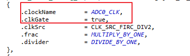
};需重点注意的地方,外设名和对应的clkGate使能,,否则外设模式时钟无法使用,从而导致外设模块无法使用,一读写相关外设模块的寄存器MCU就会跳转到复位中断后进入死循环。

5.函数调用
	CLOCK_SYS_Init(g_clockManConfigsArr, CLOCK_MANAGER_CONFIG_CNT,
                   g_clockManCallbacksArr, CLOCK_MANAGER_CALLBACK_CNT);
	CLOCK_SYS_UpdateConfiguration(0U, CLOCK_MANAGER_POLICY_FORCIBLE);
调用以上函数就可以实现时钟模块的初始化了。
6.总结
本文介绍的S32K144单片机使用SDK——clock_manager组件的配置使用,主要是结合本人在学习使用过程中觉得比较关键且容易出错的地方,即是给自己做一份备忘记录,同时希望能给有需要的朋友一点启示。


 4473
4473


 被折叠的 条评论
为什么被折叠?
被折叠的 条评论
为什么被折叠?
 到【灌水乐园】发言


