


一、概述
GPIO,即通用I/O(输入/输出)端口,是STM32可控制的引脚。STM32芯片的GPIO引脚与外部设备连接起来,可实现与外部通讯、控制外部硬件或者采集外部硬件数据的功能。STM32F407有8组IO。分别为GPIOA~GPIOH,除了GPIOH只有两个IO引脚,其余每组IO有16根引脚。
GPIO的复用:
GPIO,即通用I/O(输入/输出)端口,是STM32可控制的引脚。STM32芯片的GPIO引脚与外部设备连接起来,可实现与外部通讯、控制外部硬件或者采集外部硬件数据的功能。STM32F407有8组IO。分别为GPIOA~GPIOH,除了GPIOH只有两个IO引脚,其余每组IO有16根引脚。
二、GPIO的工作模式
1、简述
4种输入模式
(1) 浮空输入(既不连接内部上下拉电阻)
(2) 上拉输入(连接上拉电阻)
(3) 下拉输入(连接下拉电阻)
(4) 模拟输入(用于检测模拟信号的输入)
4中输出模式
(5) 开漏输出(带上拉或者下拉)
(6) 复用开漏输出(带上拉或者下拉)
(7) 推挽输出(带上拉或者下拉)
(8) 复用推挽输出(带上拉或者下拉)
4种最大输出速度
(1)2MHZ (低速)
(2)25MHZ (中速)
(3)50MHZ (快速)
(4)100MHZ (高速)
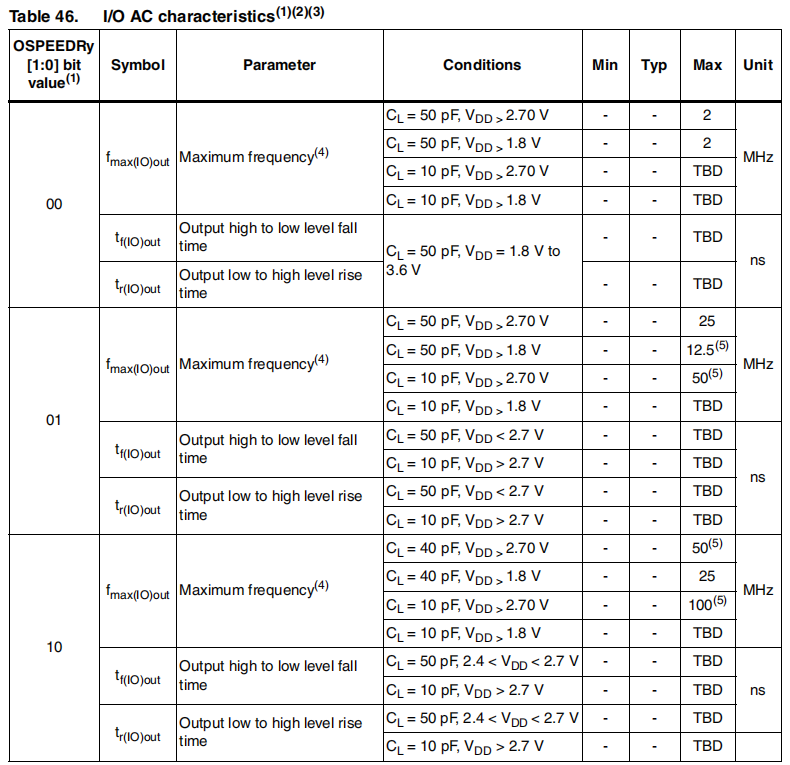
TBD:To Be Defined,被定义。

电路的驱动能力由负载电容决定的,当负载电容一定时,GPIO端口的驱动能力越大,充放电的电流也越大,上升时间就越短。另外速度越高,EMI电磁干扰就越高,因此必须平衡GPIO性能与噪声,特别是产品出口时要取得EMC(电磁兼容:Electro Magnetic Compatibility)认证。
速度越高,需要电压就越高,对应功耗也越高。
2、详细分析
输出配置
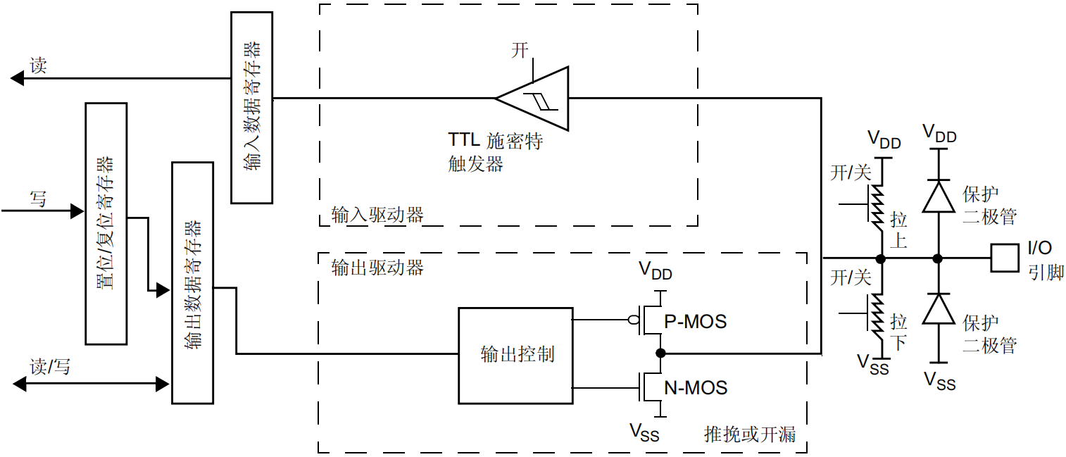
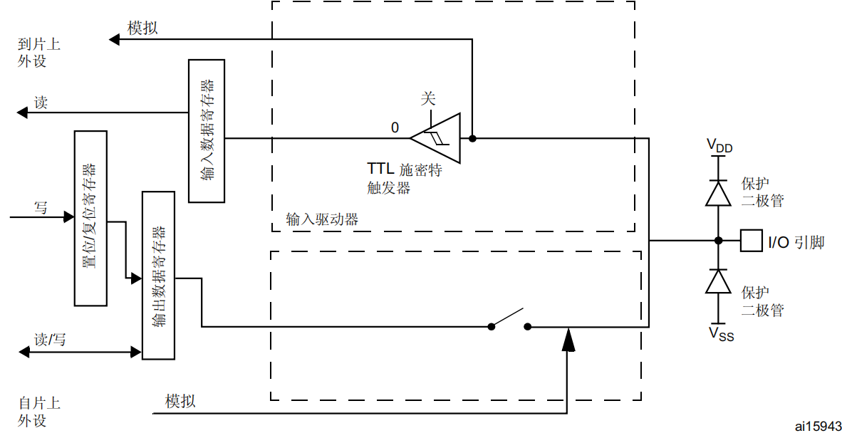
对 I/O 端口进行编程作为输出时:
- 输出缓冲器被打开:
- --开漏模式(常用于总线,典型特征是外部有上拉电阻):输出寄存器中的“0”可激活 N-MOS,而输出寄存器中的“1”会使端口保持高阻态 (Hi-Z)(P-MOS 始终不激活)
- --推挽模式:输出寄存器中的“0”可激活 N-MOS,而输出寄存器中的“1”可激活P-MOS。
- 施密特触发器输入被打开
- 根据 GPIOx_PUPDR 寄存器中的值决定是否打开弱上拉电阻和下拉电阻
- 输入数据寄存器每隔 1 个 AHB1 时钟周期对 I/O 引脚上的数据进行一次采样
- 对输入数据寄存器的读访问可获取 I/O 状态
- 对输出数据寄存器的读访问可获取最后的写入值
推挽电路(push-pull)就是两个不同极性晶体管间连接的输出电路。推挽电路采用两个参数相同的功率BJT管或MOSFET管,以推挽方式存在于电路中,各负责正负半周的波形放大任务,电路工作时,两只对称的功率开关管每次只有一个导通,所以导通损耗小效率高。推挽输出既可以向负载灌电流,也可以从负载抽取电流。
在电路设计中,推挽输出是一种很常用的输出模式。推挽输出有很多优点,比如更低的损耗,更安全的输出等。“推挽”之意,即为当一个管子推出去时,另一个管子拉回来。输入不同,交替导通。
举个例子
- 输入信号为高电平的时候,上面的管子导通,下面的管子截止,输出信号为高电平。
- 当输入信号为低电平的时候,上面的管子截止,下面的管子导通,输出信号为低电平。
MOS管
- N型mos比P型mos管使用的多
- N型mos管比P型mos管的开关速度快(工艺的影响 ),所以Pmos开关损耗多,发热严重
- Nmos比Pmos耐压高
- Nmos通过电流能力比较大,因此常用于推挽电路的下管。
输入配置
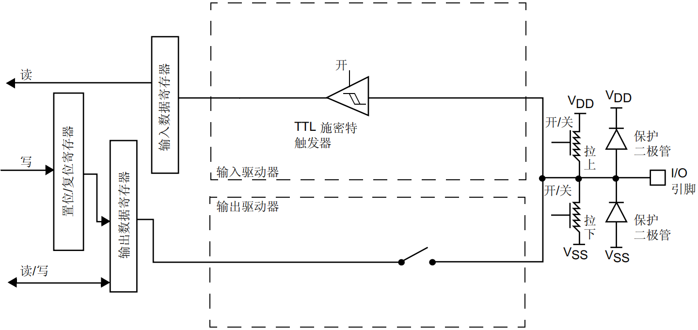
对 I/O 端口进行编程作为输入时:
- 输出缓冲器被关闭
- 施密特触发器输入被打开
- 根据 GPIOx_PUPDR 寄存器中的值决定是否打开上拉和下拉电阻
- 输入数据寄存器每隔 1 个 AHB1 时钟周期对 I/O 引脚上的数据进行一次采样
- 对输入数据寄存器的读访问可获取 I/O 状态
施密特触发器
在电子学中,施密特触发器(英语:Schmitt trigger)是包含正反馈的比较器电路。
对于标准施密特触发器,当输入电压高于正向阈值电压,输出为高;当输入电压低于负向阈值电压,输出为低;当输入在正负向阈值电压,输出不改变,也就是说输出由高电准位翻转为低电准位,或是由低点准位时所对应的阈值电压是不同的。只有当输入电压发生足够的变化时,输出才会变化,因此将这种元件命名为触发器。
施密特触发器可作为波形整形电路,能将模拟信号波形整形为数字电路能够处理的方波波形,而且由于施密特触发器具有滞回特性,所以可用于抗干扰,其应用包括在开路配置中用于抗扰,以及在闭回路正回授/负回授配置中用于实现多谐振荡器。
复用功能配置
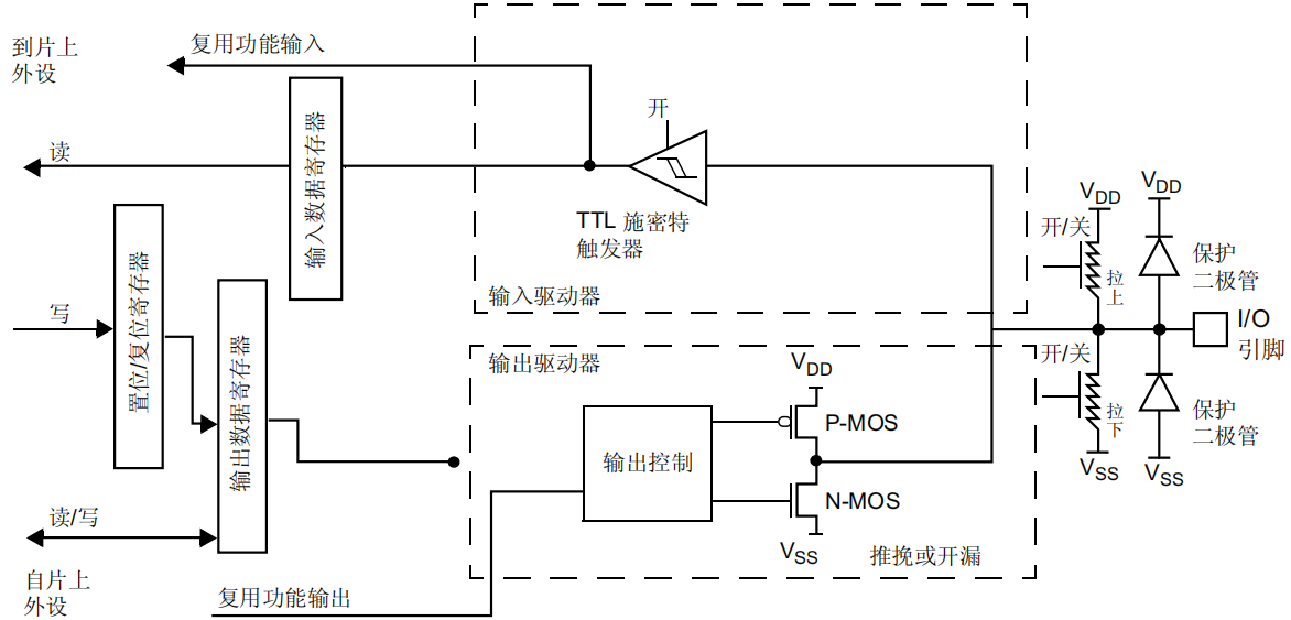
对 I/O 端口进行编程作为复用功能时:
- 可将输出缓冲器配置为开漏或推挽
- 输出缓冲器由来自外设的信号驱动(发送器使能和数据)
- 施密特触发器输入被打开
- 根据 GPIOx_PUPDR 寄存器中的值决定是否打开弱上拉电阻和下拉电阻
- 输入数据寄存器每隔 1 个 AHB1 时钟周期对 I/O 引脚上的数据进行一次采样
- 对输入数据寄存器的读访问可获取 I/O 状态
模拟配置
对 I/O 端口进行编程作为模拟配置时:
- 输出缓冲器被禁止。
- 施密特触发器输入停用,I/O 引脚的每个模拟输入的功耗变为零。施密特触发器的输出被 强制处理为恒定值 (0)。
- 弱上拉和下拉电阻被关闭。
- 对输入数据寄存器的读访问值为“0”。
在模拟配置中,I/O 引脚不能为 5 V 容忍I/O静态参数
I/O静态参数
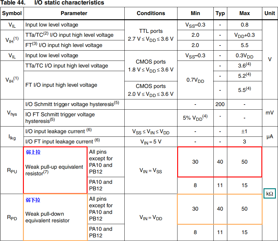
上拉电阻
1.将一个不确定的信号,通过一个电阻与电源VCC相连,固定在高电平;
2.上拉是对器件注入电流;灌电流;
3.当一个接有上拉电阻的IO端口设置为输入状态时,它的常态为高电平;
下拉电阻
1.将一个不确定的信号,通过一个电阻与地GND相连,固定在低电平;
2.下拉是从器件输出电流;拉电流;
3.当一个接有下拉电阻的IO端口设置为输入状态时,它的常态为低电平;
三、使用库函数编程技巧
1. 阅读硬件原理图《GEC-M4原理图2016-07-29.pdf》,了解当前需要使用STM32芯片哪个硬件,就可以知道使用哪些库函数接口。
2. 使用库函数的时候,只需要了解该函数的使用方法,如传入参数、返回值、功能描述就足矣。库函数里面的编写内容不需要了解,这些代码都是由ST公司去实现的。
3. 如何使用库函数实现一个具体的功能,ST公司都会提供例子文档,告诉我们库函数如何使用,如函数前后的调用顺序,详细硬件初始化流程,无论是新手还是老手都要看。
- STM32F4xx中文参考手册.pdf
- stm32f4xx_dsp_stdperiph_lib_um.chm
4. 使用的编程标准C,也就是ANSI C编程。
5. 库函数规律
- 硬件时钟 socket
- 硬件配置 bind
- 硬件控制 sendto、recvfrom
四、研究库函数
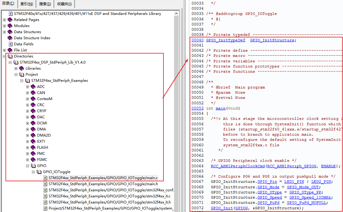
库函数参考有两种方法:
1、参考库函数源码,逐步进行阅读,仅供于参考,详细如下。
=============================================================================== ##### How to use this driver ##### ===============================================================================
(#) Enable the GPIO AHB clock using the following function RCC_AHB1PeriphClockCmd(RCC_AHB1Periph_GPIOx, ENABLE);
(#) Configure the GPIO pin(s) using GPIO_Init()
Four possible configuration are available for each pin:
(++) Input: Floating, Pull-up, Pull-down.
(++) Output: Push-Pull (Pull-up, Pull-down or no Pull) Open Drain (Pull-up, Pull-down or no Pull). In output mode, the speed is configurable: 2 MHz, 25 MHz, 50 MHz or 100 MHz.
(++) Alternate Function: Push-Pull (Pull-up, Pull-down or no Pull) Open Drain (Pull-up, Pull-down or no Pull).
(++) Analog: required mode when a pin is to be used as ADC channel or DAC output.
(#) Peripherals alternate function:
(++) For ADC and DAC, configure the desired pin in analog mode using GPIO_InitStruct->GPIO_Mode = GPIO_Mode_AN;
(+++) For other peripherals (TIM, USART...):
(+++) Connect the pin to the desired peripherals' Alternate Function (AF) using GPIO_PinAFConfig() function
(+++) Configure the desired pin in alternate function mode using GPIO_InitStruct->GPIO_Mode = GPIO_Mode_AF
(+++) Select the type, pull-up/pull-down and output speed via GPIO_PuPd, GPIO_OType and GPIO_Speed members
(+++) Call GPIO_Init() function
(#) To get the level of a pin configured in input mode use GPIO_ReadInputDataBit()
(#) To set/reset the level of a pin configured in output mode use GPIO_SetBits()/GPIO_ResetBits()
(#) During and just after reset, the alternate functions are not active and the GPIO pins are configured in input floating mode (except JTAG pins).
2.借力帮助文档
![]()
五、函数接口
1.端口硬件时钟使能
/**
* @brief Enables or disables the AHB1 peripheral clock.
* @note After reset, the peripheral clock (used for registers read/write access)
* is disabled and the application software has to enable this clock before
* using it.
* @param RCC_AHBPeriph: specifies the AHB1 peripheral to gates its clock.
* This parameter can be any combination of the following values:
* @arg RCC_AHB1Periph_GPIOA: GPIOA clock
* @arg RCC_AHB1Periph_GPIOB: GPIOB clock
* @arg RCC_AHB1Periph_GPIOC: GPIOC clock
* @arg RCC_AHB1Periph_GPIOD: GPIOD clock
* @arg RCC_AHB1Periph_GPIOE: GPIOE clock
* @arg RCC_AHB1Periph_GPIOF: GPIOF clock
* @arg RCC_AHB1Periph_GPIOG: GPIOG clock
* @arg RCC_AHB1Periph_GPIOG: GPIOG clock
* @arg RCC_AHB1Periph_GPIOI: GPIOI clock
* @arg RCC_AHB1Periph_GPIOJ: GPIOJ clock (STM32F42xxx/43xxx devices)
* @arg RCC_AHB1Periph_GPIOK: GPIOK clock (STM32F42xxx/43xxx devices)
* @arg RCC_AHB1Periph_CRC: CRC clock
* @arg RCC_AHB1Periph_BKPSRAM: BKPSRAM interface clock
* @arg RCC_AHB1Periph_CCMDATARAMEN CCM data RAM interface clock
* @arg RCC_AHB1Periph_DMA1: DMA1 clock
* @arg RCC_AHB1Periph_DMA2: DMA2 clock
* @arg RCC_AHB1Periph_DMA2D: DMA2D clock (STM32F429xx/439xx devices)
* @arg RCC_AHB1Periph_ETH_MAC: Ethernet MAC clock
* @arg RCC_AHB1Periph_ETH_MAC_Tx: Ethernet Transmission clock
* @arg RCC_AHB1Periph_ETH_MAC_Rx: Ethernet Reception clock
* @arg RCC_AHB1Periph_ETH_MAC_PTP: Ethernet PTP clock * @arg RCC_AHB1Periph_OTG_HS: USB OTG HS clock
* @arg RCC_AHB1Periph_OTG_HS_ULPI: USB OTG HS ULPI clock
* @param NewState: new state of the specified peripheral clock.
* This parameter can be: ENABLE or DISABLE.
* @retval None
*/
void RCC_AHB1PeriphClockCmd(uint32_t RCC_AHB1Periph, FunctionalState NewState)
专业英语
peripheral:英/pəˈrɪfərəl/ 外围设备;周边设备
2、GPIO的初始化
/**
* @brief Initializes the GPIOx peripheral according to the specified parameters in the GPIO_InitStruct.
* @param GPIOx: where x can be (A..K) to select the GPIO peripheral for STM32F405xx/407xx and STM32F415xx/417xx devices
* x can be (A..I) to select the GPIO peripheral for STM32F42xxx/43xxx devices.
* x can be (A, B, C, D and H) to select the GPIO peripheral for STM32F401xx devices.
* @param GPIO_InitStruct: pointer to a GPIO_InitTypeDef structure that contains
* the configuration information for the specified GPIO peripheral.
* @retval None
*/
void GPIO_Init(GPIO_TypeDef* GPIOx, GPIO_InitTypeDef* GPIO_InitStruct)
3、GPIO初始化结构体
/**
* @brief GPIO Init structure definition */
typedef struct
{
uint32_t GPIO_Pin; /*!< Specifies the GPIO pins to be configured. This parameter can be any value of @ref GPIO_pins_define */
GPIOMode_TypeDef GPIO_Mode; /*!< Specifies the operating mode for the selected pins. This parameter can be a value of @ref GPIOMode_TypeDef */
GPIOSpeed_TypeDef GPIO_Speed; /*!< Specifies the speed for the selected pins. This parameter can be a value of @ref GPIOSpeed_TypeDef */
GPIOOType_TypeDef GPIO_OType; /*!< Specifies the operating output type for the selected pins. This parameter can be a value of @ref GPIOOType_TypeDef */
GPIOPuPd_TypeDef GPIO_PuPd; /*!< Specifies the operating Pull-up/Pull down for the selected pins. This parameter can be a value of @ref GPIOPuPd_TypeDef */ }GPIO_InitTypeDef;
4.GPIO的引脚电平设置
设置高电平
/**
* @brief Sets the selected data port bits.
* @note This functions uses GPIOx_BSRR register to allow atomic read/modify
* accesses. In this way, there is no risk of an IRQ occurring between
* the read and the modify access.
* @param GPIOx: where x can be (A..K) to select the GPIO peripheral for STM32F405xx/407xx and STM32F415xx/417xx devices
* x can be (A..I) to select the GPIO peripheral for STM32F42xxx/43xxx devices.
* x can be (A, B, C, D and H) to select the GPIO peripheral for STM32F401xx devices. * @param GPIO_Pin: specifies the port bits to be written.
* This parameter can be any combination of GPIO_Pin_x where x can be (0..15).
* @retval None
*/
void GPIO_SetBits(GPIO_TypeDef* GPIOx, uint16_t GPIO_Pin)
设置低电平
/**
* @brief Clears the selected data port bits.
* @note This functions uses GPIOx_BSRR register to allow atomic read/modify
* accesses. In this way, there is no risk of an IRQ occurring between
* the read and the modify access.
* @param GPIOx: where x can be (A..K) to select the GPIO peripheral for STM32F405xx/407xx and STM32F415xx/417xx devices
* x can be (A..I) to select the GPIO peripheral for STM32F42xxx/43xxx devices.
* x can be (A, B, C, D and H) to select the GPIO peripheral for STM32F401xx devices.
* @param GPIO_Pin: specifies the port bits to be written.
* This parameter can be any combination of GPIO_Pin_x where x can be (0..15).
* @retval None
*/
void GPIO_ResetBits(GPIO_TypeDef* GPIOx, uint16_t GPIO_Pin)
设置引脚电平,可以尝试GPIO_Write、GPIO_WriteBit函数。
- 读取某个端口引脚电平
/**
* @brief Reads the specified input port pin.
* @param GPIOx: where x can be (A..K) to select the GPIO peripheral for STM32F405xx/407xx and STM32F415xx/417xx devices
* x can be (A..I) to select the GPIO peripheral for STM32F42xxx/43xxx devices.
* x can be (A, B, C, D and H) to select the GPIO peripheral for STM32F401xx devices.
* @param GPIO_Pin: specifies the port bit to read.
* This parameter can be GPIO_Pin_x where x can be (0..15).
* @retval The input port pin value.
*/
uint8_t GPIO_ReadInputDataBit(GPIO_TypeDef* GPIOx, uint16_t GPIO_Pin)
六、应用领域
1、常见密码锁,矩阵键盘


 7万+
7万+


 被折叠的 条评论
为什么被折叠?
被折叠的 条评论
为什么被折叠?
 到【灌水乐园】发言


