


一.实验目的
熟悉QUARTUSII的VHDL文本设计流程全过程,学习简单组合电路的设计,多层次电路设计,仿真和硬件测试。并实现一个二选一多路选择器。
二.实验原理:
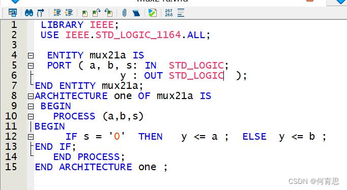
二选一多路选择器的功能描述:输入端有a,b两个输入信号,在通道控制选择控制端口s输入低电平时,输出端y输出
a信号,当s输入高电平时,输出端y输出b信号。
实验预期:当s=0,a=0,b=0,Y=0;
当s=0,a=0,b=1,Y=0;
当s=0,a=1,b=0,Y=1;
当s=0,a=1,b=1,Y=1;
当s=1,a=0,b=0,Y=0;
当s=1,a=0,b=1,Y=1;
当s=1,a=1,b=0,Y=0;
当s=1,a=1,b=1,Y=1;
三.实验过程
1.VHDL代码
代码说明:先声明三个输入端a,b,s以及一个输出端口y,然后process处理,当s输入0时,输出a,否则输出b.
2.电子元器件
四.实验结果(仿真波形图)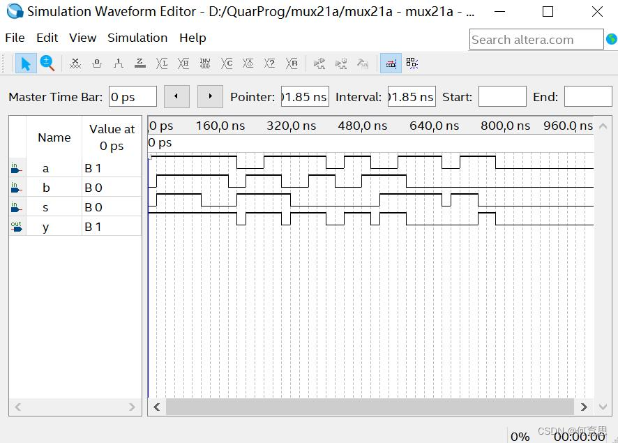
由波形图从左到右分析:
当a高电平,b低电平,s低电平时,Y高电平;当a高电平,b高电平,s高电平时,Y高电平;
当a高电平,b高电平,s低电平时,Y高电平;当a高电平,b低电平,s低电平时,Y高电平;
当a低电平,b低电平,s高电平时,Y低电平; 当a低电平,b高电平,s高电平时,Y高电平;
当a高电平,b低电平,s高电平时,Y低电平;当a低电平,b低电平,s低电平时,Y低电平;
五.实验结论
由实验结果和分析可得,当s输入高电平时,y的输出与b的输入相同;当s输入低电平时,y的输出与a的输入相同。
实验f2 一位全加器
一.实验目的:
掌握用VHDL设计简单组合电路的方法和设计流程,设计一位的全加器。
二.实验原理
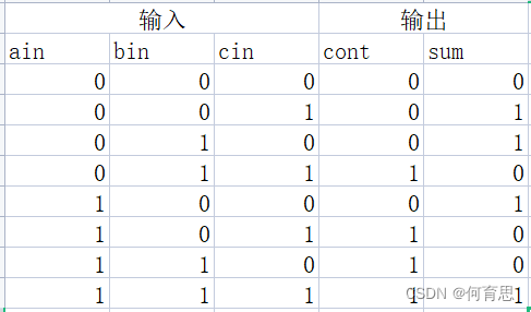
半加器设计原理:只考虑两个一位二进制数的相加,而不考虑来自低位进位数的运算电路;
其中:a、b分别为被加数与加数,作为电路的输入端,s0为两数相加产生的本位和,它和两数相加产生的向高位的进位c0一起作为电路的输出。
利用两个一位的半加器来组成一个一位的全加器。
实验预期:用ain和bin表示两个加数,cin表示低位向本位的进位,cont表示本位向高位的进位,sum表示本为和。
三.实验过程(代码图)
代码解释:ain和bin是数值输入端,cin是进位的输入端,count是进位的输出端,sum是数值输出端。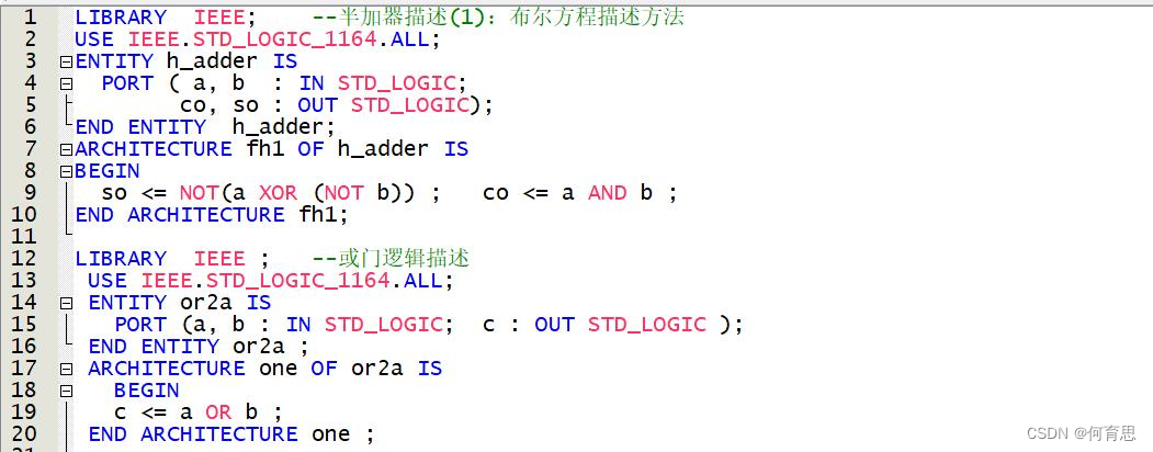

三.器件图:
四.仿真波形图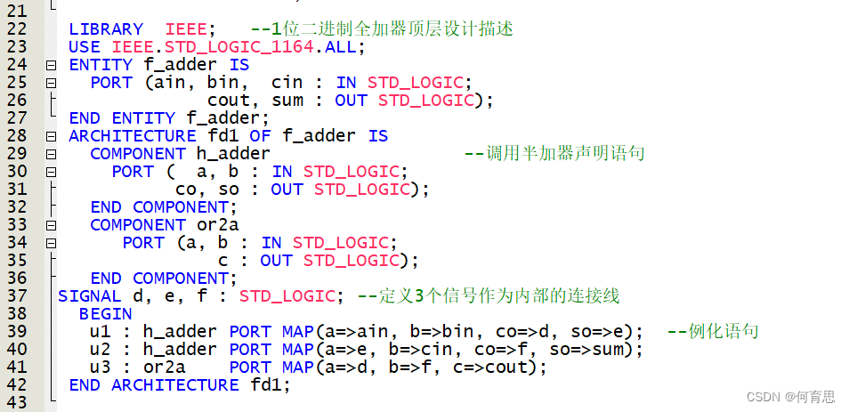
由波形图从左至右分析依次为
当ain低电平,bin高电平,cin低电平时,cout低电平,sum高电平;
当ain高电平,bin高电平,cin低电平时,cout高电平,sum低电平;
当ain高电平,bin低电平,cin高电平时,cout高电平,sum低电平;
当ain低电平,bin低电平,cin高电平时,cout低电平,sum高电平;
当ain低电平,bin高电平,cin低电平时,cout低电平,sum高电平;
当ain低电平,bin低电平,cin低电平时,cout低电平,sum低电平;
当ain高电平,bin高电平,cin高电平时,cout高电平,sum高电平;
当ain高电平,bin低电平,cin低电平时,cout低电平,sum高电平;
当ain低电平,bin高电平,cin高电平时,cout高电平,sum低电平;
五.实验结果
当输入端两个或以上为1时,cout为1,当输入端为奇数个1,sum为1,否则sum为0.
实验f3.正弦波发生器
一、实验目的
在仿真软件上完成正弦信号发生器,然后作出仿真波形图。进一步熟悉QuartusⅡ及其LPM_ROM与FPGA硬件资源的使用方法。
二、实验内容
借助ch04.ppt例4-6的例子,代码可在ppt中复制,通过视频romdemo.mp4和ppt中的初始化数据文件表格得到数据文件rom.mif,完成仿真波形图。
三.实验原理: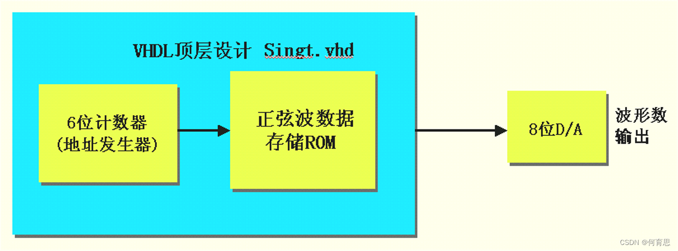
实验初始数据:
ROM数据:

LMP_ROM设计:
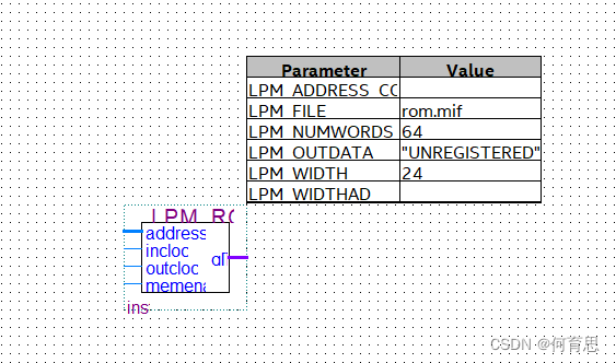
四.实验过程(实验代码)
data_rom文件,rom.mif文件,将代码和数据分别导入相应文件中,结果如下显示
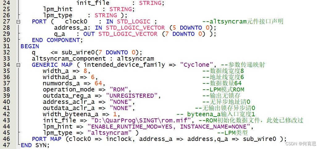
data_rom代码
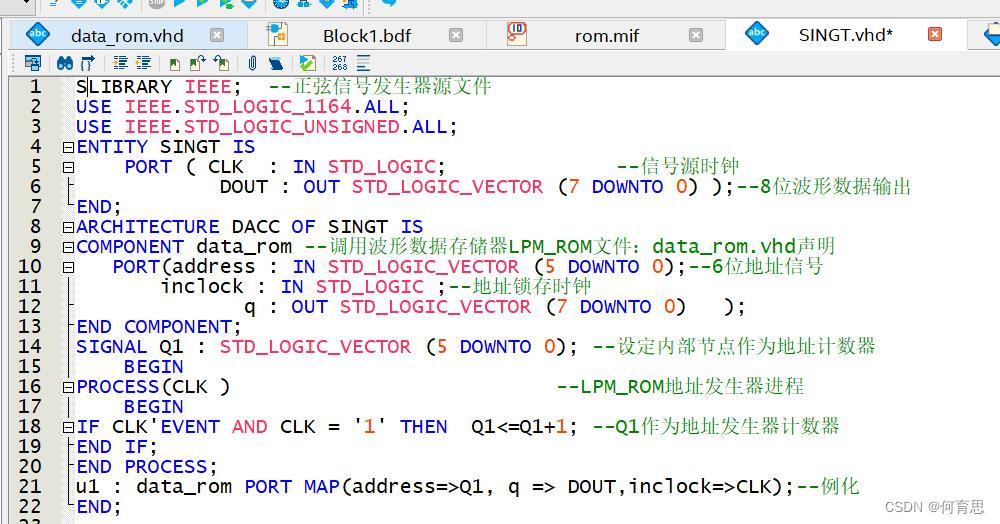
SINGT.vhd文件代码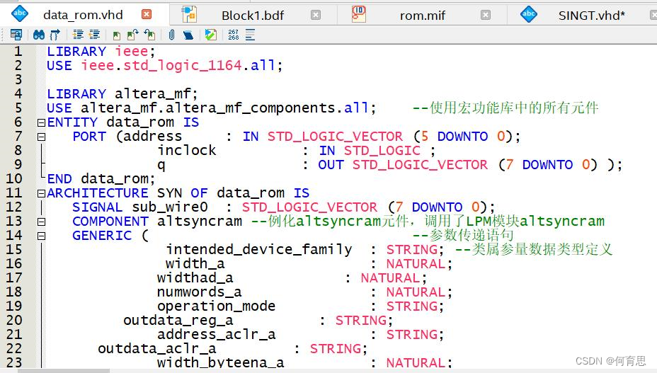
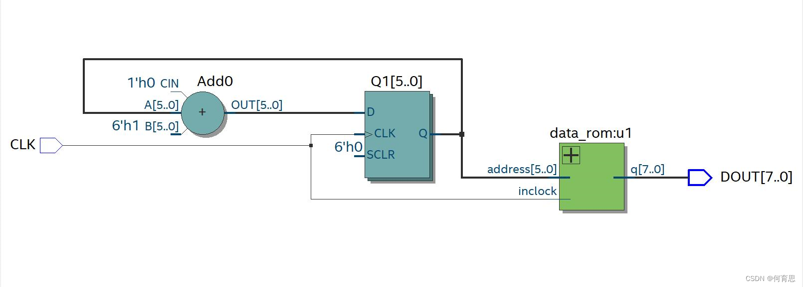
 电子元件图
电子元件图
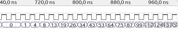
五.实验结果测试和分析:
将rom.mif文件中的数据导入data_rom.vhd文件,设定一个时钟信号20ns一个周期,仿真后得到的DOUT图如下所示,完成实验要求。

实验心得总结:
本次实验做的是正弦波信号发生器,输出仿真波形。在本次实验中除了要设计VHDL文件以外,还有.bdf .mif文件,再写VHDL时,要注意文件路径不能写错。
实验f4a 8位12指令硬布线CPU设计
一.实验目的
借助ch05.ppt,ch06.ppt和跑通范例 8位硬布线CPU设计.12条指令.doc,代码可在ppt中复制,并参考doc文件进行修改,完成仿真波形图。设计一个硬布线控制器的8位模型计算机
二.实验原理
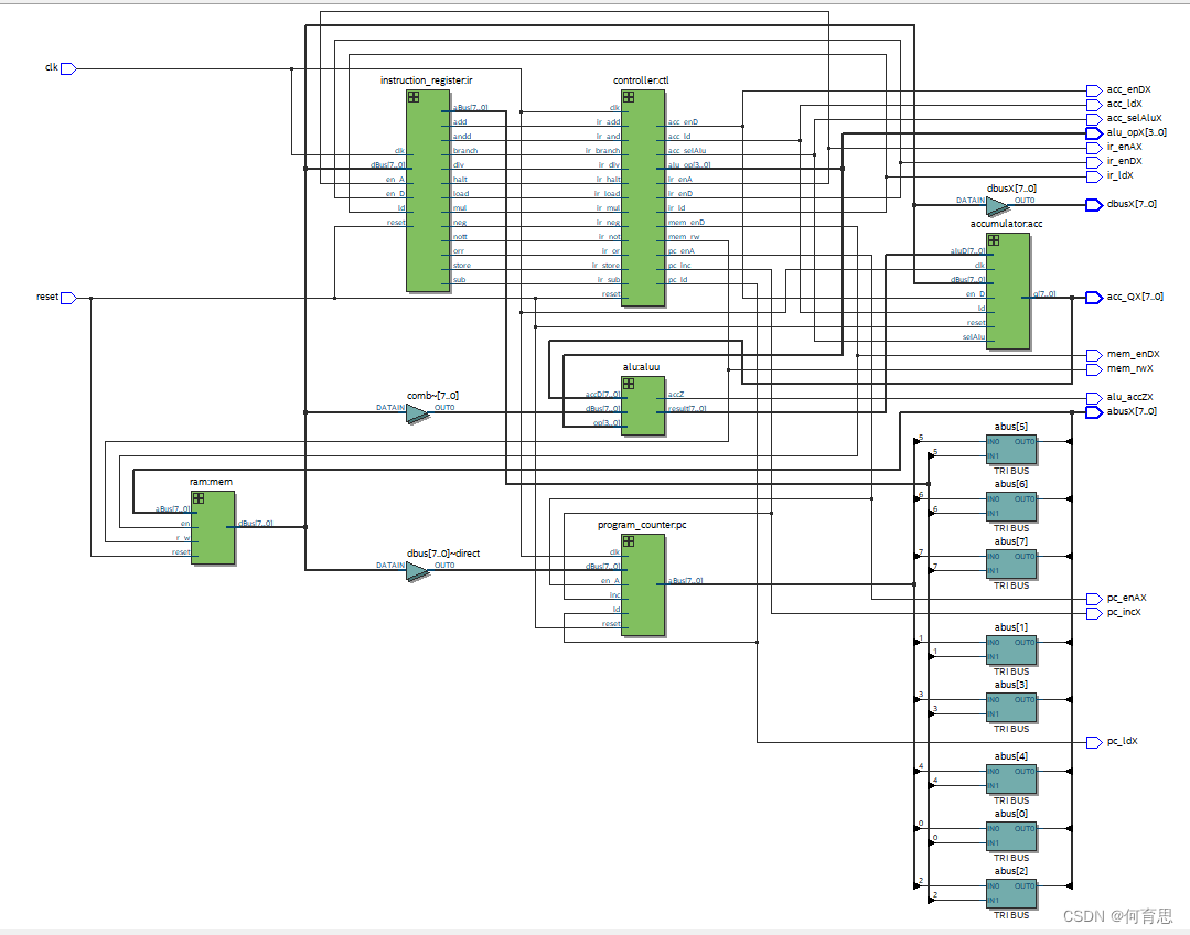
此模型计算机以控制器为中心,指令数据存储在RAM中,指令数据通过数据总线传输到指令寄存器,首先控制器从指令寄存器中取指令,编译指令,输出控制信号,控制ALU运算,PC加一,并从RAM中取出数据进行运算,运算结果寄存到累加器中,后通过数据总线存到RAM中,指令寄存器读下一条指令,依次循环。
三.实验元器件图
四.实验代码
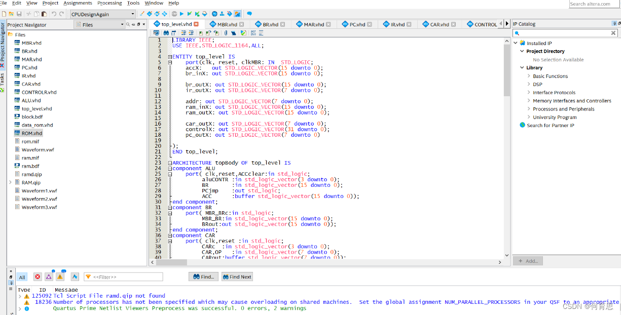
1.新建一个名为top_level的项目,分别建立top_level.vhd文件,accumulator.vhd文件,alu.vhd文件,controller.vhd文件,instruction_register.vhd文件,program_counter.vhd文件,ram.vhd文件,将代码导入相应文件中,结果如下显示。
1) top_level.vhd文件代码
library IEEE;
use IEEE.std_logic_1164.all;
entity top_level is ----声明实体外部接口
port (
clk, reset:
in STD_LOGIC;
abusX: out STD_LOGIC_VECTOR(7 downto 0); --数据总线输出
dbusX: out STD_LOGIC_VECTOR(7 downto 0);
mem_enDX, mem_rwX:
out STD_LOGIC;
pc_enAX, pc_ldX, pc_incX:
out STD_LOGIC;
ir_enAX, ir_enDX, ir_ldX:
out STD_LOGIC;
acc_enDX, acc_ldX, acc_selAluX:
out STD_LOGIC;
acc_QX: out STD_LOGIC_VECTOR(7 downto 0);
alu_accZX: out STD_LOGIC;
alu_opX: out STD_LOGIC_VECTOR(3 downto 0);
);
end top_level;
architecture topArch of top_level is
component program_counter
port (
clk, en_A, ld, inc, reset: in STD_LOGIC;
aBus: out STD_LOGIC_VECTOR(7 downto 0);
dBus: in STD_LOGIC_VECTOR(7 downto 0)
);
end component;
component instruction_register
port (
clk, en_A, en_D, ld, reset: in STD_LOGIC;
aBus: out STD_LOGIC_VECTOR(7 downto 0);
dBus: inout STD_LOGIC_VECTOR(7 downto 0);
load, store, add, sub,mul,div,andd,orr,nott,neg, halt, branch: out STD_LOGIC
);
end component;
component accumulator
port (
clk, en_D, ld, selAlu, reset: in STD_LOGIC;
aluD: in STD_LOGIC_VECTOR(7 downto 0);
dBus: inout STD_LOGIC_VECTOR(7 downto 0);
q: out STD_LOGIC_VECTOR(7 downto 0)
);
end component;
component alu
port (
op: in STD_LOGIC_VECTOR(3 downto 0);
accD: in STD_LOGIC_VECTOR(7 downto 0);
dBus: in STD_LOGIC_VECTOR(7 downto 0);
result: out STD_LOGIC_VECTOR(7 downto 0);
accZ: out STD_LOGIC
);
end component;
component ram
port (
r_w, en, reset: in STD_LOGIC;
aBus: in STD_LOGIC_VECTOR(7 downto 0);
dBus: inout STD_LOGIC_VECTOR(7 downto 0)
);
end component;
component controller
port (
clk, reset: in STD_LOGIC;
mem_enD, mem_rw: out STD_LOGIC;
pc_enA, pc_ld, pc_inc: out STD_LOGIC;
ir_enA, ir_enD, ir_ld: out STD_LOGIC;
ir_load, ir_store, ir_add: in STD_LOGIC;
ir_sub, ir_mul, ir_div: in STD_LOGIC;
ir_and, ir_or, ir_not: in STD_LOGIC;
ir_neg, ir_halt, ir_branch: in STD_LOGIC;
acc_enD, acc_ld, acc_selAlu: out STD_LOGIC;
alu_op: out STD_LOGIC_VECTOR(3 downto 0)
);
end component;
signal abus: STD_LOGIC_VECTOR(7 downto 0);
signal dbus: STD_LOGIC_VECTOR(7 downto 0);
signal mem_enD, mem_rw: STD_LOGIC;
signal pc_enA, pc_ld, pc_inc: STD_LOGIC;
signal ir_enA, ir_enD, ir_ld: STD_LOGIC;
signal ir_load, ir_store, ir_add: STD_LOGIC;
signal ir_sub, ir_mul, ir_div: STD_LOGIC;
signal ir_and, ir_or, ir_not: STD_LOGIC;
signal ir_negate, ir_halt, ir_branch: STD_LOGIC;
signal acc_enD, acc_ld, acc_selAlu: STD_LOGIC;
signal acc_Q: STD_LOGIC_VECTOR(7 downto 0);
signal alu_op: STD_LOGIC_VECTOR(3 downto 0);
signal alu_accZ: STD_LOGIC;
signal alu_result: STD_LOGIC_VECTOR(7 downto 0);
begin
pc: program_counter port map(clk, pc_enA, pc_ld, pc_inc, reset, abus, dbus);
ir: instruction_register port map(clk, ir_enA, ir_enD, ir_ld, reset, abus,dbus,ir_load,ir_store,ir_add,ir_sub,ir_mul,ir_div,ir_and,ir_or,ir_not,ir_negate, ir_halt, ir_branch );
acc: accumulator port map(clk, acc_enD, acc_ld, acc_selAlu, reset, alu_result, dbus, acc_Q);
aluu: alu port map(alu_op, acc_Q, dbus, alu_result, alu_accZ);
mem: ram port map(mem_rw, mem_enD, reset, abus, dbus);
ctl: controller port map (
clk, reset, mem_enD, mem_rw, pc_enA, pc_ld, pc_inc,
ir_enA, ir_enD, ir_ld, ir_load, ir_store, ir_add,ir_sub,
ir_mul,ir_div,ir_and,ir_or,ir_not,
ir_negate, ir_halt, ir_branch,acc_enD,
acc_ld, acc_selAlu, alu_op
);
abusX <= abus;
dbusX <= dbus;
mem_enDX <= mem_enD;
mem_rwX <= mem_rw;
pc_enAX <= pc_enA;
pc_ldX <= pc_ld;
pc_incX <= pc_inc;
ir_enAX <= ir_enA;
ir_enDX <= ir_enD;
ir_ldX <= ir_ld;
acc_enDX <= acc_enD;
acc_ldX <= acc_ld;
acc_selAluX <= acc_selAlu;
acc_QX <= acc_Q;
alu_opX <= alu_op;
alu_accZX <= alu_accZ;
end topArch;
2)accumulator.vhd文件代码
library IEEE;
use IEEE.std_logic_1164.all;
use IEEE.std_logic_unsigned.all;
entity accumulator is ----声明外部实体接口
port (
clk, en_D, ld, selAlu, reset: in STD_LOGIC; --时钟信号
aluD: in STD_LOGIC_VECTOR(7 downto 0);
dBus: inout STD_LOGIC_VECTOR(7 downto 0);
q: out STD_LOGIC_VECTOR(7 downto 0)
);
end accumulator;
architecture accArch of accumulator is
signal accReg: STD_LOGIC_VECTOR(7 downto 0);
begin
process(clk) begin
if clk'event and clk = '1' then
if reset = '1' then
accReg <= "00000000";
elsif ld = '1' and selAlu = '1' then
accReg <= aluD;
elsif ld = '1' and selAlu = '0' then
accReg <= dBus;
end if;
end if;
end process;
dBus <= accReg when en_D = '1' else
"ZZZZZZZZ";
q <= accReg;
end accArch;
3)alu.vhd文件代码
library IEEE;
use IEEE.std_logic_1164.all;
use IEEE.std_logic_unsigned.all;
entity alu is -----实体声明外部接口
port (
op: in STD_LOGIC_VECTOR(3 downto 0); --选择控制运算类型
accD: in STD_LOGIC_VECTOR(7 downto 0); -- 累加器的8位数据
dBus: in STD_LOGIC_VECTOR(7 downto 0); -- 数据总线用于运算
result: out STD_LOGIC_VECTOR(7 downto 0); --结果的输出
accZ: out STD_LOGIC
);
end alu;
architecture aluArch of alu is
begin
result <= (not accD) + "00000001" when op ="0000" else
accD + dBus when op ="0001" else
accD+"10000000" when op="0010" else
dBus+"10000000" when op="0011" else
(not accD)-"00000001" when op="0100" else
accD-dBus when op="0101" else
accD(3 downto 0)*dBus(3 downto 0) when op="0110" else
--accD*dBus when op="0110" else
--accD(3 downto 0)*(Not dBus(3 downto 0)) when op="0111" else
accD(3 downto 0)*(NOT dBus(3 downto 0)) when op="0111" else
accD AND dBus when op="1010" else
accD NAND dBus when op="1011" else
accD OR dBus when op="1100" else
accD NOR dBus when op="1101" else
accD XNOR dBus when op="1110" else
NOT accD when op="1111" else
"00000000";
accZ <= not (accD(0) or accD(1) or accD(2) or accD(3) or
accD(4) or accD(5) or accD(6) or accD(7)
);
end aluArch;
4)controller.vhd文件代码
library IEEE;
use IEEE.std_logic_1164.all;
entity controller is ----声明实体外部接口
port (
clk, reset:
in STD_LOGIC;
mem_enD, mem_rw:
out STD_LOGIC;
pc_enA, pc_ld, pc_inc: out STD_LOGIC;
ir_enA, ir_enD, ir_ld: out STD_LOGIC;
ir_load, ir_store, ir_add: in STD_LOGIC;
ir_sub,ir_mul,ir_div: in STD_LOGIC;
ir_and,ir_or, ir_not: in STD_LOGIC;
ir_neg, ir_halt, ir_branch: in STD_LOGIC;
acc_enD, acc_ld, acc_selAlu: out STD_LOGIC;
alu_op: out STD_LOGIC_VECTOR(3 downto 0)
);
end controller;
architecture controllerArch of controller is
type state_type is ( reset_state,
fetch0, fetch1,
load0, load1,
store0, store1,
add0, add1,
sub0, sub1,
mul0, mul1,
div0, div1,
and0, and1,
or0, or1,
not0, not1,
negate0, negate1,
halt,
branch0, branch1
);
signal state: state_type;
begin
process(clk) begin
if clk'event and clk = '1' then
if reset = '1' then state <= reset_state;
else
case state is
when reset_state => state <= fetch0;
when fetch0 => state <= fetch1;
when fetch1 =>
if ir_load = '1' then state <= load0;
elsif ir_store = '1' then state <= store0;
elsif ir_add = '1' then state <= add0;
elsif ir_sub = '1' then state <= sub0;
elsif ir_mul = '1' then state <= mul0;
elsif ir_div = '1' then state <= div0;
elsif ir_and = '1' then state <= and0;
elsif ir_or = '1' then state <= or0;
elsif ir_not = '1' then state <= not0;
elsif ir_neg = '1' then state <= negate0;
elsif ir_halt = '1' then state <= halt;
elsif ir_branch = '1' then state <= branch0;
end if;
when load0 => state <= load1;
when load1 => state <= fetch0;
when store0 => state <= store1;
when store1 => state <= fetch0;
when add0 => state <= add1;
when add1 => state <= fetch0;
when sub0 => state <= sub1;
when sub1 => state <= fetch0;
when mul0 => state <= mul1;
when mul1 => state <=fetch0;
when div0 => state <=div1;
when div1 => state <=fetch0;
when and0 => state <=and1;
when and1 => state <=fetch0;
when or0 => state <=or1;
when or1 => state <=fetch0;
when not0 => state <=not1;
when not1 => state <=fetch0;
when negate0 => state <= negate1;
when negate1 => state <= fetch0;
when halt => state <= halt;
when branch0 => state <= branch1;
when branch1 => state <= fetch0;
when others => state <= halt;
end case;
end if;
end if;
end process;
process(clk) begin -- special process for memory write timing
if clk'event and clk = '0' then
if state = store0 then
mem_rw <= '0';
else
mem_rw <= '1';
end if;
end if;
end process;
mem_enD <= '1' when state = fetch0 or state = fetch1 or
state = load0 or state = load1 or
state = add0 or state = add1 or
state = sub0 or state = sub1 or
state = mul0 or state = mul1 or
state = div0 or state = div1 or
state = and0 or state = and1 or
state = or0 or state = or1 else '0';
pc_enA <= '1' when state = fetch0 or
state = fetch1 else '0';
pc_ld <= '1' when state = branch0
else '0';
pc_inc <= '1' when state = fetch1
else '0';
ir_enA <= '1' when state = load0 or
state = load1 or state = store0 or
state = store1 or state = add0 or
state = add1 or state = sub0 or
state = sub1 or state = mul0 or
state = mul1 or state = div0 or
state = div1 or state = and0 or
state = and1 or state = or0 or
state = or1 else '0';
ir_enD <= '1' when state = branch0
else '0';
ir_ld <= '1' when state = fetch1
else '0';
acc_enD <= '1' when state = store0 or state = store1 else '0';
acc_ld <= '1' when state = load1 or state = add1 or state = negate1
or state = sub1 or state = mul1 or state = div1
or state = not1 or state = or1 or state = not1 else '0';
acc_selAlu <='1' when state = add1 or state = negate1 or state = sub1 or
state = mul1 or state = div1 or state = not1 or
state = or1 or state = not1 else '0';
alu_op <= "0001" when state = add0 or state = add1
else "0101" when state = sub0 or state = sub1
else "0110" when state = mul0 or state = mul1
else "0111" when state = div0 or state = div1
else "0000" when state = negate0 or state = negate1
else "1010" when state = and0 or state = and1
else "1100" when state = or0 or state = or1
else "1111" when state = not0 or state = not1;
--alu_op <= "01" when state = add0 or state = add1 else "00";
end controllerArch;
5)instruction_register.vhd文件代码
library IEEE;
use IEEE.std_logic_1164.all;
entity instruction_register is ----声明实体外部接口
port (
clk, en_A, en_D, ld, reset: in STD_LOGIC;
aBus: out STD_LOGIC_VECTOR(7 downto 0); ----数据总线输出
dBus: inout STD_LOGIC_VECTOR(7 downto 0);
load, store, add, sub,mul,div,andd,orr,nott,neg, halt, branch: out STD_LOGIC
);
end instruction_register;
architecture irArch of instruction_register is
signal irReg: STD_LOGIC_VECTOR(7 downto 0);
begin
process(clk) begin
if clk'event and clk = '0' then -- load on falling edge
if reset = '1' then
irReg <= "00000000";
elsif ld = '1' then
irReg <= dBus;
end if;
end if;
end process;
aBus <= "0000" & irReg(3 downto 0) when en_A = '1' else
"ZZZZZZZZ";
dBus <= "0000" & irReg(3 downto 0) when en_D = '1' else
"ZZZZZZZZ";
load <= '1' when irReg(7 downto 4) = "0000" else '0';
store <= '1' when irReg(7 downto 4) = "0001" else '0';
add <= '1' when irReg(7 downto 4) = "0010" else '0';
sub <= '1' when irReg(7 downto 4) = "0011" else '0';
mul <= '1' when irReg(7 downto 4) = "0100" else '0';
div <= '1' when irReg(7 downto 4) = "0101" else '0';
neg <= '1' when irReg = "0110" & "0000" else '0';
andd <= '1' when irReg (7 downto 4) = "0111" else '0';
orr <= '1' when irReg (7 downto 4) = "1000" else '0';
nott <= '1' when irReg (7 downto 4) = "1001" else '0';
halt <= '1' when irReg = "1010" & "0001" else '0';
branch <= '1' when irReg(7 downto 4) = "1011" else '0';
end irArch;
6)program_counter.vhd文件代码
library IEEE;
use IEEE.std_logic_1164.all;
use IEEE.std_logic_unsigned.all;
entity program_counter is
port (
clk, en_A, ld, inc, reset: in STD_LOGIC;
aBus: out STD_LOGIC_VECTOR(7 downto 0); --数据总线输出
dBus: in STD_LOGIC_VECTOR(7 downto 0) --数据总线输入
);
end program_counter;
architecture pcArch of program_counter is
signal pcReg: STD_LOGIC_VECTOR(7 downto 0);
begin
process(clk) begin
if clk'event and clk = '1' then
if reset = '1' then
pcReg <= "00000000";
elsif ld = '1' then
pcReg <= dBus;
elsif inc = '1' then
pcReg <= pcReg + "00000001";
end if;
end if;
end process;
aBus <= pcReg when en_A = '1' else "ZZZZZZZZ";
end pcArch;
7)ram。Vhd文件代码
library IEEE;
use IEEE.std_logic_1164.all;
use IEEE.std_logic_arith.all;
entity ram is
port (
r_w, en, reset: in STD_LOGIC;
aBus: in STD_LOGIC_VECTOR(7 downto 0); ----数据总线输入
dBus: inout STD_LOGIC_VECTOR(7 downto 0)
);
end ram;
architecture ramArch of ram is
type ram_typ is array(0 to 63) of STD_LOGIC_VECTOR(7 downto 0);
signal ram: ram_typ;
begin
process(
en, reset, r_w, aBus, dBus
) begin
if reset = '1' then
ram(0) <= x"14"; --00010100 store 0100
ram(1) <= x"30"; --00110000 sub 0000
ram(2) <= x"25"; --00100101 add 0101
ram(3) <= x"15"; --00010101 store 0101
ram(4) <= x"46"; --01000110 mul 0110
ram(5) <= x"31"; --00110001 sub 0001
ram(6) <= x"55"; --01010101 div 0101
ram(7) <= x"06"; --00000110 load 0110
ram(8) <= x"01"; --00000001 load 0001
elsif r_w = '0' then
ram(conv_integer(unsigned(aBus))) <= dBus;
end if;
end process;
dBus <= ram(conv_integer(unsigned(aBus)))
when reset = '0' and en = '1' and r_w = '1' else
"ZZZZZZZZ";
end ramArch;
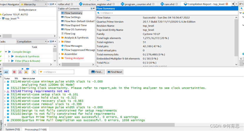
2. 编译运行
五.实验结果
波形图

实验分析:
| 序号 | 指令字 | 汇编指令 |
| 1 | ram(0) <= x"14"; | STORE 1 |
| 2 | ram(1) <= x"30"; | SUB 3 |
| 3 | ram(2) <= x"25"; | ADD 2 |
| 4 | ram(3) <= x"15"; | STORE 1 |
| 5 | ram(4) <= x"00"; | LOAD 4 |
| 6 | ram(5) <= x"1D"; | STORE 1 |
| 7 | ram(6) <= x"55"; | DIV 5 |
| 8 | ram(7) <= x"06"; | LOAD 0 |
| 9 | ram(8) <= x"01"; | LOAD 0 |
结果显示9条指令的地址和操作如红圈部分所示。其中:
指令1:PC=0,从总线得到指令14(H),指令分为操作码和地址两部分。其中操作码为1,表示store操作,4为4号单元地址,将acc中的值00存入该单元,此时4号地址单元值为00。操作完成,PC自动+1。
指令2:PC=1,从总线得到指令30(H),指令分为操作码和地址两部分。其中操作码为3,表示sub操作,0为0号单元地址,将acc中的值减去0号单元中的数值14(H),减后结果为EC(H)存入acc中,操作完成,PC自动+1。
指令3:PC=2,从总线得到指令25(H),指令分为操作码和地址两部分。其中操作码为2,表示add操作,5为5号单元地址,将acc中的值加上5号单元中的数值31(H),相加结果为1D(H)存入acc中,操作完成,PC自动+1。
指令4:PC=3,从总线得到指令15(H),指令分为操作码和地址两部分。其中操作码为1,表示store操作,5为5号单元地址,将acc中的值1D存入5号单元中,此时5号地址单元值为1D。操作完成,PC自动加1。
指令5:PC=4,从数据总线得到指令00(H),指令分为操作码和地址两部分。其中操作码为0,表示load操作,0为0号单元地址,将0号单元的值14(H)存入acc中,操作完成,PC自动+1。
指令6:PC=5,从总线得到指令1D(H),指令分为操作码和地址两部分。其中操作码为1,表示store操作,D为D号单元地址,将acc中的值14(H)存入D号单元中,此时D号地址单元值为14(H)。操作完成,PC自动+1。
指令7:PC=6,从总线得到指令55(H),指令分为操作码和地址两部分。其中操作码为5,表示div操作,5为5号单元地址,,将acc中的值14(H)除以5号单元中的值1D(H),相除结果向下取整为0,存入acc中。操作完成,PC自动+1。
指令8:PC=7,从总线得到指令06(H),指令分为操作码和地址两部分。其中操作码为0,表示load操作,6为6号单元地址,即将6号单元中的值55(H)存入acc中,此时acc中的值为55(H)。操作完成,PC自动+1。
指令9:PC=8,从总线得到指令01(H),指令分为操作码和地址两部分。其中操作码为0,表示load操作,1为1号单元地址,即将1号单元的值30(H)存入acc中,此时acc中的值为30(H)。操作完成。
指令1为store指令,即将acc中的数据存到相应内存单元中。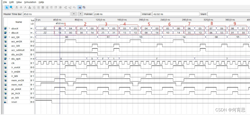
ir从地址总线中取得指令14(H),此时pc_enA=1,且PC=PC+1,此时men_rw=1,还未将acc中相应数据传入内存单元中,当men_rw=0,开始进行数据写入操作,即4号地址单元中得到acc中的数值,操作完成。
后面的操作与上述过程类似,不再一一复述。
六.实验总结与思考
通过这次实验f4a:8位12指令硬布线CPU设计,.通过这个实验加深了对VHDL语言的理解和印象,同时对CPU设计的相关知识有更进一步的认识和学习。
实验f4b 8位12指令微程序CPU设计
一.实验目的
在仿真软件上完成8位12微指令CPU设计,然后做出仿真波形图。
借助ch05.ppt,ch06.ppt和跑通范例 8位微程序CPU设计_包含程序.12条指令.doc,代码可在ppt中复制,并参考doc文件进行修改,完成仿真波形图。
二.实验设计
此微程序CPU由MRR,MAR,PC,IR,CAR,CONTROLD,ALU,ROM,RAM组成。其中各功能如下
MBR存储器缓冲存储器,从RAM读取的微程序寄存到MBR中,经过MBR解析出指令码和操作数据,分别通过指令寄存器和缓冲寄存器传输到ALU中进行运算;同时ALU运算的结果寄存到MBR中,通过写入操作,将运算结果写入到RAM中。ACC_MBRc控制MBR读取ALU得到的结果ACC,将ACC传输到MBR寄存,当R为1,为读操作,MBR从RAM中读取数据,当W为1时,MBR将ALU寄存的结果传输到RAM进行存储,MBR_MAR为传输到MAR的地址码,MBR_PC为传输到PC的地址码,地址码都来源于RAM存储的程序的前8位。MBR_OPc控制读取RAM中程序的操作码,为RAM存储的程序的后8位。
MAR是存储器地址寄存器,用来解析出机器指令在RAM中的地址,当PC_MARc为1时,按照程序计数器输出的指令地址在RAM中查找对应的位置;当MBR_MARc为1时,按照MBR输出的指令地址在RAM中查找对应位置。
PC程序计数器,获取下一条指令在RAM中的地址,该地址可以通过当前地址加1得到下一指令的地址,也可以通过来自MBR的输出得到下一指令地址。CONTRalu在PC中是用来判断ALU是否被访问,若CONTRalu没有被访问,则通过PCjmp是控制程序计数器获取指令地址的方式,若PCjmp为1,下一指令地址通过MBR获得,若为0,则通过程序计数器加1获取。PCcl控制程序计数器置零,PCinc控制程序计数器进行加1操作,PCc3是控制程序计数器从MBR中获取指令地址。
IR指令寄存器,寄存微程序的操作码,输出的opcode输入到CAR中,用于获取微指令的地址。
CAR控制地址寄存器,用于获取微指令在ROM中的地址。CARc控制获取微指令地址的寻址方式。在该代码中,分别有基址变址寻址、直接寻址以及自增寻址。当使用基址变址寻址时,从IR输出的OP与CAR中寄存的地址进行相加,获取微指令在ROM中的地址。当使用使用直接寻址时,直接通过控制器CONTROLR输出的微指令地址。当使用自增寻址时,通过CAR中寄存的地址进行加1获取微指令地址。
CONTROLD控制器,通过ROM输出的微指令,对微指令进行解码,获取各控制指令。
ALU运算器,对BR传来的数据和累加器ACC中寄存的数据进行运算,aluCONIR控制ALU的运算操作,当ACC中的数据不为0时,控制程序计数器从MBR获取操作数的地址,反之,程序计数器加1获取下一指令地址。
ROM存储各种微指令,与RAM同样通过IP核进行构建,通过mif文件写入微指令代码。
三.实验生成图
器件图

布局图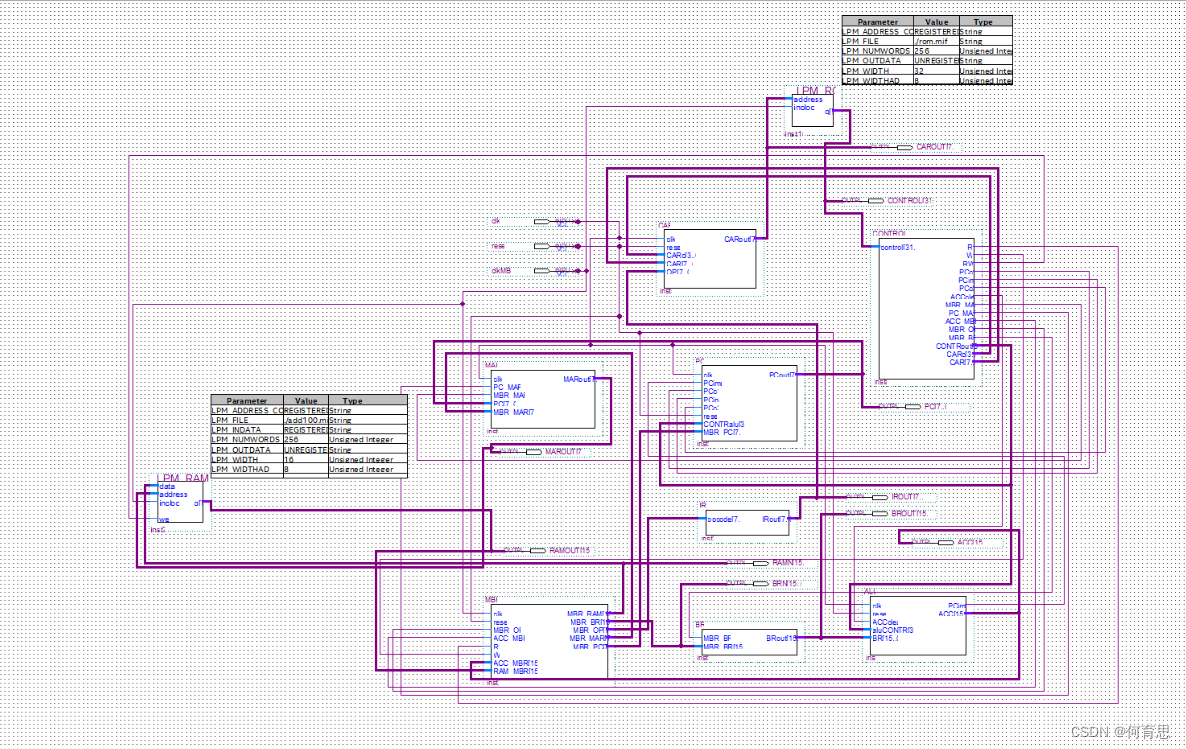
四.实验过程
新建一个名为top_level的项目,分别建立top_level.vhd文件,MBR.vhd文件,BR.vhd文件,MAR.vhd文件,PC.vhd文件,IR.vhd文件,CAR.vhd文件,CONTRALR.vhd文件,ALU.vhd文件,LMP_ROM.vhd文件,LMP_RAM.vhd文件,block_bdf文件,rom.mif文件,ram.mif文件将代码导入相应文件中,结果如下显示。
实验代码如下:
(1)top_level.vhd
LIBRARY IEEE;
USE IEEE.STD_LOGIC_1164.ALL;
ENTITY top_level IS
port(clk, reset, clkMBR: IN STD_LOGIC;
accX: out STD_LOGIC_VECTOR(15 downto 0);
br_inX: out STD_LOGIC_VECTOR(15 downto 0);
br_outX: out STD_LOGIC_VECTOR(15 downto 0);
ir_outX: out STD_LOGIC_VECTOR(7 downto 0);
addr: out STD_LOGIC_VECTOR(7 downto 0);
ram_inX: out STD_LOGIC_VECTOR(15 downto 0);
ram_outX: out STD_LOGIC_VECTOR(15 downto 0);
car_outX: out STD_LOGIC_VECTOR(7 downto 0);
controlX: out STD_LOGIC_VECTOR(31 downto 0);
pc_outX: out STD_LOGIC_VECTOR(7 downto 0)
);
END top_level;
ARCHITECTURE topBody OF top_level IS
component ALU
port( clk,reset,ACCclear:in std_logic;
aluCONTR :in std_logic_vector(3 downto 0);
BR :in std_logic_vector(15 downto 0);
PCjmp :out std_logic;
ACC :buffer std_logic_vector(15 downto 0));
end component;
component BR
port( MBR_BRc:in std_logic;
MBR_BR:in std_logic_vector(15 downto 0);
BRout:out std_logic_vector(15 downto 0));
end component;
component CAR
port( clk,reset :in std_logic;
CARc :in std_logic_vector(3 downto 0);
CAR,OP :in std_logic_vector(7 downto 0);
CARout:buffer std_logic_vector(7 downto 0));
end component;
component CONTROLR
port(
control :in std_logic_vector(31 downto 0);
R,W, RW, PCc1,PCinc,PCc3:out std_logic;
ACCclear,MBR_MARc,PC_MARc:out std_logic;
ACC_MBRc,MBR_OPc,MBR_BRc:out std_logic;
CONTRout:out std_logic_vector(3 downto 0);
CARc :out std_logic_vector(3 downto 0);
CAR :out std_logic_vector(7 downto 0));
end component;
component IR
port( opcode :in std_logic_vector(7 downto 0);
IRout :out std_logic_vector(7 downto 0));
end component;
component MAR
port( clk,PC_MARc,MBR_MARc:in std_logic;
PC,MBR_MAR:in std_logic_vector(7 downto 0);
MARout:out std_logic_vector(7 downto 0));
end component;
component MBR
port( clk, reset, MBR_OPc, ACC_MBRc,R,W:in std_logic;
ACC_MBR :in std_logic_vector(15 downto 0);
RAM_MBR :in std_logic_vector(15 downto 0);
MBR_RAM :out std_logic_vector(15 downto 0);
MBR_BR :out std_logic_vector(15 downto 0);
MBR_OP :out std_logic_vector(7 downto 0);
MBR_MAR :out std_logic_vector(7 downto 0);
MBR_PC :out std_logic_vector(7 downto 0));
end component;
component PC
port( clk,PCjmp,PCc1,PCinc,PCc3,reset:in std_logic;
CONTRalu :in std_logic_vector(3 downto 0);
MBR_PC :in std_logic_vector(7 downto 0);
PCout :buffer std_logic_vector(7 downto 0));
end component;
component RAM
PORT (
address : IN STD_LOGIC_VECTOR (7 DOWNTO 0);
clock : IN STD_LOGIC;
data : IN STD_LOGIC_VECTOR (15 DOWNTO 0);
wren : IN STD_LOGIC ;
q : OUT STD_LOGIC_VECTOR (15 DOWNTO 0));
end component;
COMPONENT data_rom
PORT(address : IN STD_LOGIC_VECTOR (7 DOWNTO 0);
inclock : IN STD_LOGIC ;
q : OUT STD_LOGIC_VECTOR (31 DOWNTO 0)
);
END COMPONENT;
signal pc_jmp: std_logic;
signal acc: std_logic_vector(15 downto 0);
signal br_out: std_logic_vector(15 downto 0);
signal car_out: std_logic_vector(7 downto 0);
signal ir_out: std_logic_vector(7 downto 0);
signal mar_out: std_logic_vector(7 downto 0);
signal ram_out: std_logic_vector(15 downto 0);
signal rom_out: std_logic_vector(31 downto 0);
signal mbr_ram: std_logic_vector(15 downto 0);
signal mbr_br: std_logic_vector(15 downto 0);
signal mbr_op: std_logic_vector(7 downto 0);
signal mbr_mar: std_logic_vector(7 downto 0);
signal mbr_pc: std_logic_vector(7 downto 0);
signal pc_out: std_logic_vector(7 downto 0);
signal r: std_logic;
signal w: std_logic;
signal rw: std_logic;
signal pcc1: std_logic;
signal pcinc: std_logic;
signal pcc3: std_logic;
signal acc_clear: std_logic;
signal mbr_marc: std_logic;
signal pc_marc: std_logic;
signal acc_mbrc: std_logic;
signal mbr_opc: std_logic;
signal mbr_brc: std_logic;
signal controut: std_logic_vector(3 downto 0);
signal car_c: std_logic_vector(3 downto 0);
signal car_o: std_logic_vector(7 downto 0);
begin
aluu: ALU port map (clk, reset, acc_clear, controut, br_out, pc_jmp, acc);
brr: BR port map (mbr_brc, mbr_br, br_out);
carr: CAR port map (clk, reset, car_c, car_o, ir_out, car_out);
controler: CONTROLR port map (rom_out, r, w, rw, pcc1, pcinc, pcc3, acc_clear, mbr_marc, pc_marc,acc_mbrc,mbr_opc,mbr_brc,controut,car_c, car_o);
irr: IR port map (mbr_op, ir_out);
marr: MAR port map (clk, pc_marc, mbr_marc, pc_out, mbr_mar, mar_out);
mbrr: MBR port map (clkMBR, reset, mbr_opc, acc_mbrc, r, w, acc, ram_out, mbr_ram, mbr_br, mbr_op, mbr_mar, mbr_pc);
pcc: PC port map (clk, pc_jmp, pcc1, pcinc, pcc3, reset, controut, mbr_pc, pc_out);
ramm: RAM port map (mar_out, clk, mbr_ram, rw, ram_out);
romm: data_rom port map (car_out, clk, rom_out);
accX<=acc;
br_inX<=mbr_br;
br_outX<=br_out;
ir_outX<=ir_out;
ram_inX<=mbr_ram;
addr<=mar_out;
ram_outX<=ram_out;
car_outX<=car_out;
controlX<=rom_out;
pc_outX<=pc_out;
END topBody;
(2)MBR.vhd
library ieee;
use ieee.std_logic_1164.all;
use ieee.std_logic_unsigned.all;
entity MBR is
port( clk, reset, MBR_OPc, ACC_MBRc,R,W:in std_logic;
ACC_MBR :in std_logic_vector(15 downto 0);
RAM_MBR :in std_logic_vector(15 downto 0);
MBR_RAM :out std_logic_vector(15 downto 0);
MBR_BR :out std_logic_vector(15 downto 0);
MBR_OP :out std_logic_vector(7 downto 0);
MBR_MAR :out std_logic_vector(7 downto 0);
MBR_PC :out std_logic_vector(7 downto 0));
end MBR;
architecture behave of MBR is
begin
process(clk)
variable temp:std_logic_vector(15 downto 0);
begin
if(clk'event and clk='0')then
if reset='1' then
if ACC_MBRc='1' then temp:=ACC_MBR; end if;
if R='1' then MBR_BR<=RAM_MBR; end if;
if W='1' then MBR_RAM<=temp; end if;
MBR_MAR<=RAM_MBR(7 downto 0);
MBR_PC<=RAM_MBR(7 downto 0);
if MBR_OPc='1' then MBR_OP<=RAM_MBR(15 downto 8); end if;
else MBR_BR<=x"0000";
MBR_MAR<="00000000";
MBR_OP<="00000000";
MBR_PC<="00000000";
end if;
end if;
end process;
end behave;
(3)BR.vhd
library ieee;
use ieee.std_logic_1164.all;
entity BR is
port( MBR_BRc:in std_logic;
MBR_BR:in std_logic_vector(15 downto 0);
BRout:out std_logic_vector(15 downto 0));
end BR;
architecture behave of BR is
begin
process(MBR_BRc)
begin
if MBR_BRc='1' then BRout<=MBR_BR; end if;
end process;
end behave;
(4)MAR.vhd
library ieee;
use ieee.std_logic_1164.all;
use ieee.std_logic_unsigned.all;
entity MAR is
port( clk,PC_MARc,MBR_MARc:in std_logic;
PC,MBR_MAR:in std_logic_vector(7 downto 0);
MARout:out std_logic_vector(7 downto 0));
end MAR;
architecture behave of MAR is
begin
process(clk)
begin
if(clk'event and clk='1')then
if PC_MARc='1' then MARout<=PC; end if;
if MBR_MARc='1' then MARout<=MBR_MAR; end if;
end if;
end process;
end behave;
(5)PC.vhd
library ieee;
use ieee.std_logic_1164.all;
use ieee.std_logic_unsigned.all;
entity PC is
port( clk,PCjmp,PCc1,PCinc,PCc3,reset:in std_logic;
CONTRalu :in std_logic_vector(3 downto 0);
MBR_PC :in std_logic_vector(7 downto 0);
PCout :buffer std_logic_vector(7 downto 0));
end PC;
architecture behave of PC is
begin
process(clk)
begin
if(clk'event and clk='0')then
if reset='1' then
if CONTRalu="0101" then
if PCjmp='1' then PCout<=MBR_PC;
elsif PCjmp='0' then PCout<=PCout+1;
end if;
end if;
if PCc1='1' then PCout<="00000000"; end if;
if PCinc='1' then PCout<=PCout+1; end if;
if PCc3='1' then PCout<=MBR_PC; end if;
else PCout<="00000000";
end if;
end if;
end process;
end behave;
(6)IR.vhd
library ieee;
use ieee.std_logic_1164.all;
use ieee.std_logic_unsigned.all;
entity IR is
port( opcode :in std_logic_vector(7 downto 0);
IRout :out std_logic_vector(7 downto 0));
end IR;
architecture behave of IR is
begin
IRout<=opcode;
end behave;
(7)CAR.vhd
library ieee;
use ieee.std_logic_1164.all;
use ieee.std_logic_unsigned.all;
entity CAR is
port( clk,reset :in std_logic;
CARc :in std_logic_vector(3 downto 0);
CAR,OP :in std_logic_vector(7 downto 0);
CARout:buffer std_logic_vector(7 downto 0));
end CAR;
architecture behave of CAR is
begin
process(clk)
begin
if(clk'event and clk='1')then
if reset='1' then
if CARc="1000" then CARout<="00000000"; end if;
if CARc="0100" then CARout<=OP+CARout; end if;
if CARc="0010" then CARout<=CAR; end if;
if CARc="0001" then CARout<=CARout+1; end if;
else CARout<="00000000";
end if;
end if;
end process;
end behave;
(8)CONTROLR.vhd
library ieee;
use ieee.std_logic_1164.all;
use ieee.std_logic_unsigned.all;
entity CONTROLR is
port(
control :in std_logic_vector(31 downto 0);
R,W, RW, PCc1,PCinc,PCc3:out std_logic;
ACCclear,MBR_MARc,PC_MARc:out std_logic;
ACC_MBRc,MBR_OPc,MBR_BRc:out std_logic;
CONTRout:out std_logic_vector(3 downto 0);
CARc :out std_logic_vector(3 downto 0);
CAR :out std_logic_vector(7 downto 0));
end CONTROLR;
architecture behave of CONTROLR is
begin
process(control)
begin
CAR<=control(7 downto 0);
PCc1<=control(8);
PCinc<=control(9);
PCc3<=control(10);
ACCclear<=control(11);
CONTRout<=control(15 downto 12);
R<=control(16);
W<=control(17);
MBR_MARc<=control(18);
PC_MARc<=control(19);
ACC_MBRc<=control(20);
MBR_OPc<=control(21);
MBR_BRc<=control(22);
CARc<=control(26 downto 23);
RW<=control(17);
end process;
end behave;
(9)ALU.vhd
library ieee;
use ieee.std_logic_1164.all;
use ieee.std_logic_unsigned.all;
entity ALU is
port( clk,reset,ACCclear:in std_logic;
aluCONTR :in std_logic_vector(3 downto 0);
BR :in std_logic_vector(15 downto 0);
PCjmp :out std_logic;
ACC :buffer std_logic_vector(15 downto 0));
end ALU;
architecture behave of ALU is
begin
process(clk)
begin
if(clk'event and clk='0')then
if reset='0' then ACC<=x"0000";
else
if ACCclear='1' then ACC<=x"0000"; end if;
if aluCONTR="0011" then ACC<=BR+ACC; end if; --ADD
if aluCONTR="0100" then ACC<=ACC-BR; end if; --SUB
if aluCONTR="0110" then ACC<=ACC and BR; end if; --AND
if aluCONTR="0111" then ACC<=ACC or BR; end if; --OR
if aluCONTR="1000" then ACC<=not ACC; end if; --NOT
if aluCONTR="1001" then --SRR
ACC(14 downto 0)<=ACC(15 downto 1); ACC(15)<='0';
end if;
if aluCONTR="1010" then --SRL
ACC(15 downto 1)<=ACC(14 downto 0); ACC(0)<='0';
end if;
if aluCONTR="1011" then ACC<=ACC + BR;
end if; --MPY
end if;
end if;
if ACC>0 then PCjmp<='1';
else PCjmp<='0';
end if;
end process;
end behave;
(10)LMP_ROM.vhd
LIBRARY ieee;
USE ieee.std_logic_1164.all;
LIBRARY altera_mf;
USE altera_mf.altera_mf_components.all; --使用宏功能库中的所有元件
ENTITY LMP_ROM IS
PORT (address : IN STD_LOGIC_VECTOR (7 DOWNTO 0);
inclock : IN STD_LOGIC ;
q : OUT STD_LOGIC_VECTOR (31 DOWNTO 0) );
END data_rom;
ARCHITECTURE SYN OF data_rom IS
SIGNAL sub_wire0 : STD_LOGIC_VECTOR (31 DOWNTO 0);
COMPONENT altsyncram --例化altsyncram元件,调用了LPM模块altsyncram
GENERIC ( --参数传递语句
intended_device_family : STRING; --类属参量数据类型定义
width_a : NATURAL;
widthad_a : NATURAL;
numwords_a : NATURAL;
operation_mode : STRING;
outdata_reg_a : STRING;
address_aclr_a : STRING;
outdata_aclr_a : STRING;
width_byteena_a : NATURAL;
init_file : STRING;
lpm_hint : STRING;
lpm_type : STRING );
PORT ( clock0 : IN STD_LOGIC ; --altsyncram元件接口声明
address_a: IN STD_LOGIC_VECTOR (7 DOWNTO 0);
q_a : OUT STD_LOGIC_VECTOR (31 DOWNTO 0) );
END COMPONENT;
BEGIN
q <= sub_wire0(31 DOWNTO 0);
altsyncram_component : altsyncram
GENERIC MAP ( intended_device_family => "Cyclone", --参数传递映射
width_a => 32, --数据线宽度8
widthad_a => 8, --地址线宽度6
numwords_a => 128, --数据数量64
operation_mode => "ROM", --LPM模式ROM
outdata_reg_a => "UNREGISTERED", --输出无锁存
address_aclr_a => "NONE", --无异步地址清0
outdata_aclr_a => "NONE", --无输出锁存异步清0
width_byteena_a => 1, -- byteena_a输入口宽度1
init_file => "./rom.mif", --ROM初始化数据文件,此处已修改过
lpm_hint => "ENABLE_RUNTIME_MOD=YES, INSTANCE_NAME=NONE",
lpm_type => "altsyncram" ) --LPM类型
PORT MAP (clock0 => inclock, address_a => address,q_a => sub_wire0 );
END SYN;
(11)LMP_RAM.vdl
LIBRARY ieee;
USE ieee.std_logic_1164.all;
LIBRARY altera_mf;
USE altera_mf.altera_mf_components.all;
ENTITY LMP_RAM IS
PORT
(
address : IN STD_LOGIC_VECTOR (7 DOWNTO 0);
data : IN STD_LOGIC_VECTOR (15 DOWNTO 0);
inclock : IN STD_LOGIC := '1';
wren : IN STD_LOGIC ;
q : OUT STD_LOGIC_VECTOR (15 DOWNTO 0)
);
END RAM;
ARCHITECTURE SYN OF ram IS
SIGNAL sub_wire0 : STD_LOGIC_VECTOR (15 DOWNTO 0);
BEGIN
q <= sub_wire0(15 DOWNTO 0);
altsyncram_component : altsyncram
GENERIC MAP (
clock_enable_input_a => "BYPASS",
clock_enable_output_a => "BYPASS",
init_file => "./data/ram4.mif",
intended_device_family => "Cyclone IV GX",
lpm_hint => "ENABLE_RUNTIME_MOD=NO",
lpm_type => "altsyncram",
numwords_a => 256,
operation_mode => "SINGLE_PORT",
outdata_aclr_a => "NONE",
outdata_reg_a => "UNREGISTERED",
power_up_uninitialized => "FALSE",
read_during_write_mode_port_a => "NEW_DATA_NO_NBE_READ",
widthad_a => 8,
width_a => 16,
width_byteena_a => 1
)
PORT MAP (
address_a => address,
clock0 => inclock,
data_a => data,
wren_a => wren,
q_a => sub_wire0
);
END SYN;
(12)ram.mif文件

(13)rom.mif文件
五.实验结果
设定时钟信号clk 20ns一个周期,clkMBR 20ns一个周期,reset设置完后,仿真,得到以下波形图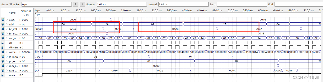
结果分析:以上述圈红的两条指令为例进行相关数据分析如下
1.从总线上得到指令022A,指令分为操作码和地址吗,其中操作码为02,表示Load操作,2A为2A号单元地址,将2A号单元的值0016(H)存入acc中,操作完成。
2.从总线上得到指令042B,指令分为操作码和地址吗,其中操作码为04,表示SUB操作,2B为2B号单元地址,将acc中的值减去2B号单元中的数值000A(H),减后结果存入acc中,操作完成。
六、实验心得
1.实验中给予我们所参考的doc文件中缺少顶层设计文件和相关数据导入的文件,在编译过程中根据提醒来进行修改,花费了不少的时间,同时和同学共同探讨,对PPT内容以及去搜索相关资料后才知道如何去设计顶层代码,去录入相关数据,在不断的试错中发现解决方案,最后在同学们的帮助下共同完成了顶层设计文件,得出相应的波形图和RTL图。
2.通过这个实验加深了对VHDL语言的理解和印象,在f4a实验的基础上更加深入了解到CPU的工作机制,同时实验的难度也是较大, 感谢对我给予帮助的同学的帮助和指点,我将在未来的学习生活中打磨自己的耐心和技术,也感谢老师给予的机会,能学习到这些相关内容。


 3327
3327


 被折叠的 条评论
为什么被折叠?
被折叠的 条评论
为什么被折叠?
 到【灌水乐园】发言


