


 本文介绍了模拟电子线路的核心概念,包括半导体的性质、晶体管的类型及其工作原理,重点讲解了PN结、半波整流和齐纳二极管的应用,以及共射放大电路的工作机制。同时提到了运算放大器在信号处理中的作用。
模拟电子线路
Analog circuit
需要熟悉课程名,一句话简单概括课程内容,准备一些重点内容介绍。
-
This course mainly introduces the properties(n.性质) of semiconductors(半导体) and transistors, and then analyzes and masters amplification circuits.
-
Semiconductors (e.g. Si, Ge) are materials whose conductivity is between an insulator(n.绝缘体) (e.g. dry wood) and a conductor (e.g. iron, water).
When impurities(n.杂质) are added, the conductivity(n.导电能力) of semiconductors changes. Semiconductors can be classified two types:
N-type semiconductors: It mainly uses electrons to conduct electricity.
P-type semiconductors: It mainly uses holes to conduct electricity.
Majority carriers(多数载流子)
Minority carriers(少数载流子) -
When these 2 types semiconductors contact, holes and electrons will recombine, and then will form an intermediate region called PN junction.
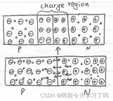
When diffusion motion and charge region reach balance, the width of PN junction will not change.
If an electric field is added, this balance is disrupted(v.破坏).
If we add Forward bias(正向偏置) electric field, diffusion motion will become strong, and then form forward current. PN junction will become shorter.
When the voltage is large enough, PN junction conduct.
If we add Reverse bias(反向偏置) electric field, the space charge region will become wide, diffusion motion become difficult and only minority carriers can move. PN junction will become wider.
When the voltage is large enough, the current barely passes, called cut-off state. -
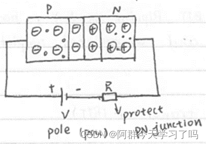
When PN junction add a shell(n.外壳), a diode is formed.
Voltage-current characteristics of a diode is like this:
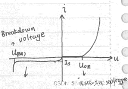
Different materials have different conduct voltage: Silicon: 0.7V; Germanium(锗): 0.3V.
Two classic applications: half-wave rectification, Zener diode(齐纳二极管).
Half-wave rectification:
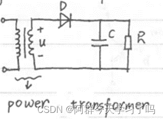
This circuit can change the alternating current(AC.交流电) to the direct current(DC. 直流电).
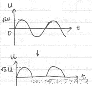
The half wave can pass, another half wave can’t pass.
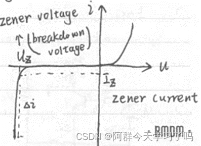
Zener diode works on reverse breakdown(反向击穿), on a certain current range, the voltage almost doesn’t change.
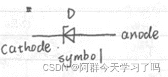
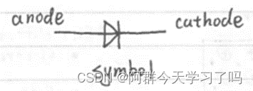
Anode: 阳极; cathode: 阴极. -
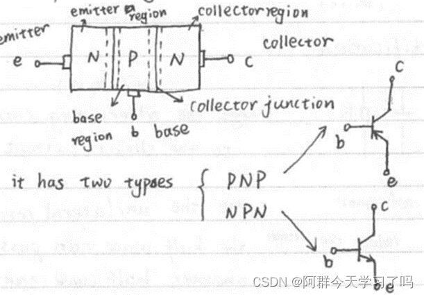
If we use two PN junction, we can form triode transistor (BJT).
It’s an important element for amplify circuit and it can amplify current.
Depending on the applied voltage, it has 3 work regions:
- Cut-off region: the emitter junction voltage weaker than cut-in voltage and collector junction reverse bias.
- Amplifier region: the emitter junction forward bias and collector junction reverse bias.
- Saturation region: the emitter junction and collector junction forward bias.
- Basic amplifying circuits:
Basic common-emitter amplify circuit is like this:
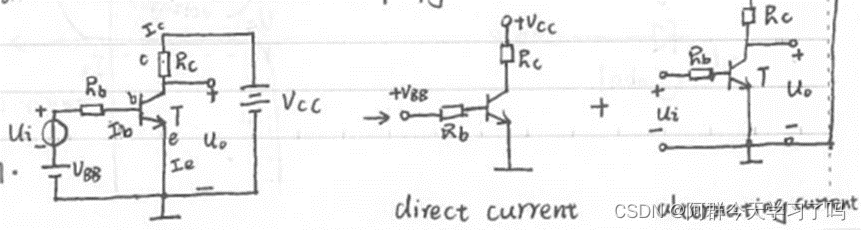
- When Ui=0, the amplifying circuit is in static state.
The VBB makes the Ube> Uon, the VCC makes the collector junction reverse bias, so the triode transistor will work on amplify state.
IC=βIB, for RC, the Uc= IC* RC, so Uce=Vcc- IC* RC. - When Ui≠0, it will produce dynamic current ib, ic.
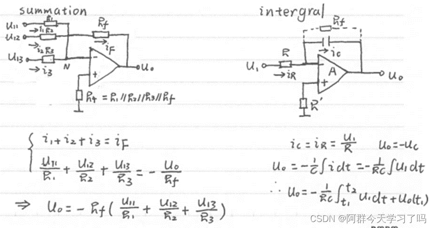
- Operational amplifying circuits(运算放大电路)
It’s used to the operation of many analog signal, such as summation(求和), integral(积分), differencing(差分).


 836
836


 被折叠的 条评论
为什么被折叠?
被折叠的 条评论
为什么被折叠?
 到【灌水乐园】发言


