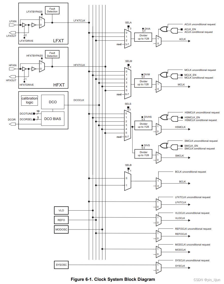
MSP432-系统时钟简介

MSP432Pxx-系统时钟框图简介

                                                        SEL为选择器,DIV为分频器

外部时钟源       

        LFXT为外部低速时钟源,HFXT为外部高速时钟源,均需要外接晶振

内部时钟源

        DCO数控时钟源,默认频率为3MHz,可通过程序改变频率,使用内部电阻时精度不高,

        可外接精密电阻使用,通过DCO可以时钟超频至64MHz。(超频有风险,试玩需谨慎)

        VLO超低功耗低频时钟源,典型频率为9.4KHz。

        REFO低频时钟源,典型频率为32768Hz和128KHz。

        MODOSC模块振荡器,典型频率为25MHz。可做ADC时钟源,采样频率1M

        SYSOSC系统震荡器,典型频率为5MHz。可做ADC时钟源,采样频率200K

时钟来源

        ACLK为辅助时钟,最大时钟频率128KHz,可为各外设提供时钟来源。

        MCLK为主时钟,可选择六个时钟源,CPU和滴答定时器即是接在这个时钟上的。

        HSMCLK子系统时钟和  SMCLK低速子系统时钟均是给外设使用的。

        BCLK低速备用时钟,最大时钟频率限制在32768Hz。

默认时钟设置

        当系统reset后或者不进行时钟配置时,会进入内核电压0的模式,等级0的最大时钟

        频率为24MHz。

        此时ACLKBCLK都是选择LFXTCLK作为时钟输入,但此时LFXTCLK是禁用的,

        LFXT的晶振输入输出引脚此时为通用I/O,需要启用此时钟需要复用端口,所以系统

        认为LFXT故障,选择REFOCLK作为时钟来源,此时时钟频率为32768Hz。

        外部高速时钟源HFXT也不启用,此时MCLK, HSMCLK, SMCLK时钟来源都是DCO

        数控时钟源,此时时钟频率都为3MHz。

时钟故障机制

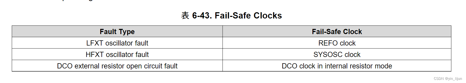
 Fault Type下时钟源故障后会选择Fail-Safe Clock里的时钟源。

最后一条DCO外接精密电阻故障即开路或者短路时会启用内部电阻,但不精确。

  • 2
    点赞
  • 9
    收藏
    觉得还不错? 一键收藏
  • 0
    评论
MSP432 低功耗高性能并存10.1 Digital I/O Introduction The digital I/O features include: • Independently programmable individual I/Os • Any combination of input or output • Individually configurable interrupts for ports (available for certain ports only) • Independent input and output data registers • Individually configurable pullup or pulldown resistors • Wake-up capability from ultra-low power modes (available for certain ports only) • Individually configurable high drive I/Os (available for certain I/Os only) Devices within the family may have up to eleven digital I/O ports implemented (P1 to P10 and PJ). Most ports contain eight I/O lines; however, some ports may contain less (see the device-specific data sheet for ports available). Each I/O line is individually configurable for input or output direction, and each can be individually read or written. Each I/O line is individually configurable for pullup or pulldown resistors. Certain ports have interrupt and wake-up capability from ultra-low power modes (see device specific data sheet for ports with interrupt and wake-up capability). Each interrupt can be individually enabled and configured to provide an interrupt on a rising or falling edge of an input signal. All interrupts are fed into an encoded Interrupt Vector register, allowing the application to determine which sub-pin of a port has generated the event. Individual ports can be accessed as byte-wide ports or can be combined into half-word-wide ports. Port pairs P1 and P2, P3 and P4, P5 and P6, P7 and P8, and so on, are associated with the names PA, PB, PC, PD, and so on, respectively. All port registers are handled in this manner with this naming convention. The main exception are the interrupt vector registers, for example, interrupts for ports P1 and P2 must be handled through P1IV and P2IV, PAIV does not exist. When writing to port PA with half-word operations, all 16 bits are written to the port. When writing to the lower byte of port PA using byte operations,

“相关推荐”对你有帮助么?

  • 非常没帮助
  • 没帮助
  • 一般
  • 有帮助
  • 非常有帮助
提交
评论
添加红包

请填写红包祝福语或标题

红包个数最小为10个

红包金额最低5元

当前余额3.43前往充值 >
需支付:10.00
成就一亿技术人!
领取后你会自动成为博主和红包主的粉丝 规则
hope_wisdom
发出的红包
实付
使用余额支付
点击重新获取
扫码支付
钱包余额 0

抵扣说明:

1.余额是钱包充值的虚拟货币,按照1:1的比例进行支付金额的抵扣。
2.余额无法直接购买下载,可以购买VIP、付费专栏及课程。

余额充值