


1. 加号 +
1.1 使用verilog编程,如下:
module adder(
	input 		[1:0]				din,
	input 		[1:0]				din_1,
	output		[2:0]				DOUT,
);
 assign DOUT=din+din_1;
endmodule
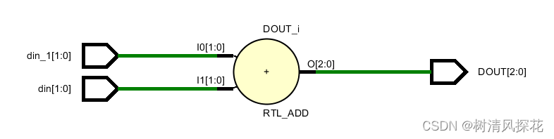
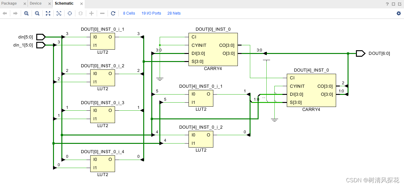
1.2 RTL 分析后的原理图:
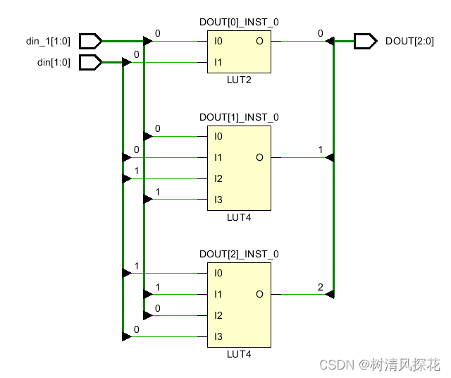
1.3 综合后的原理图:
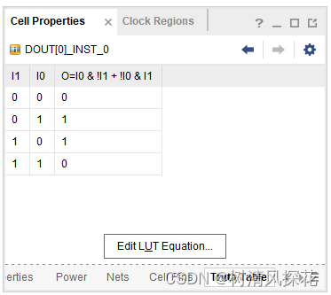
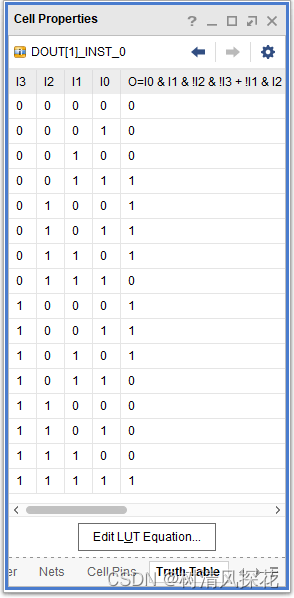
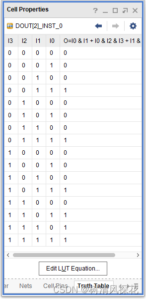
1.4 LUT的真值表:
下图中:DOUT[0]_INST_0的真值表逻辑关系与异或门的逻辑关系一致;
器件资源使用情况,仅使用LUT资源
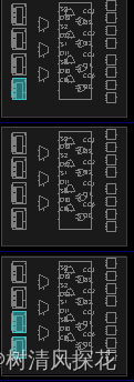
1.5 布线
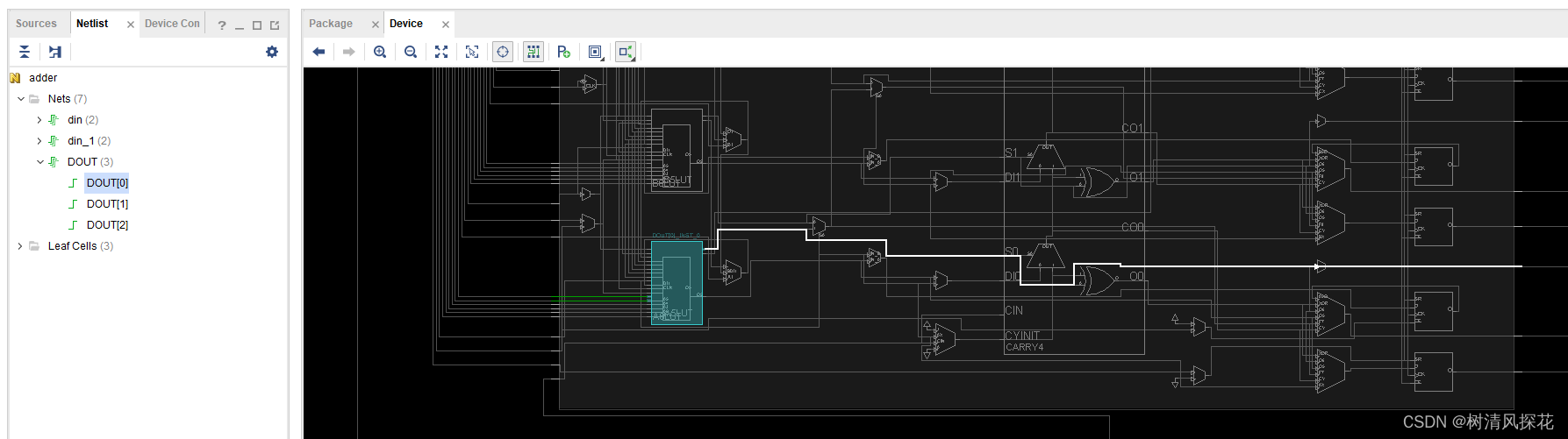

1.6 网表文件
生成网表文件步骤:
- 设置synthesis option 中的 -flatten_hierarchy为full(意味着模块综合后的层级结构为平级);
- 设置synthesis option 中的 more options为-mode out_of_context(意味着网表不插入IOBUF);
- 生成*.v例化文件 write_verilog -mode synth_stub E:/adder.v
- 生成*_sim.v仿真顶层文件 write_verilog -mode funcsim -force E:/adder_sim.v
- 生成网表文件:不包含IP核:write_edif E:/adder.edf
- 生成网表文件:包含IP核:write_edif -security_mode all E:/adder.edf
(instance (rename DOUT_0__INST_0 "DOUT[0]_INST_0") (viewref netlist (cellref LUT2 (libraryref hdi_primitives)))
           (property INIT (string "4'h6"))
         )
(instance (rename DOUT_1__INST_0 "DOUT[1]_INST_0") (viewref netlist (cellref LUT4 (libraryref hdi_primitives)))
           (property INIT (string "16'h8778"))
         )
(instance (rename DOUT_2__INST_0 "DOUT[2]_INST_0") (viewref netlist (cellref LUT4 (libraryref hdi_primitives)))
           (property INIT (string "16'hE888"))
         )
LUT2:DOUT[0]_INST_0:初始化值4’h6=4’b0110,与真值表的输出一致;4’b0110 从右至左数,第0位等于1’b0、第1位等于1’b1、第2位等于1’b1、第3位等于1’b0<==>一行真值表的输入从左往右组合,一列真值表的输出从上往下组合;
当{din[1],din[0]}等于2‘b01(din[1]等于1‘b0、din[0]等于1‘b1)或等于2’b10(din[1]等于1‘b1、din[0]等于1‘b0)时,DOUT[0]_INST_0输出为1,其余组合输出为0。
当{din[0],din[1]}等于1或等于2时,LUT2的初始化值从右至左从0开始数到第1位、第2位输出为1。
LUT的输入相当于地址线,当{I0,I1}满足LUT初始化值的位置关系时,LUT输出为1。
以DOUT[2]_INST_0为例:当DOUT[2]_INST_0输入为4‘h1110时,DOUT[2]_INST_0的输出为高还是低?
解: 4‘h1110=14;
DOUT[2]_INST_0初始值16’hE888=16’b1110100010001000;
初始值的第14位等于1‘b1;
所以当DOUT[2]_INST_0输入为4‘h1110时,DOUT[2]_INST_0的输出为高。
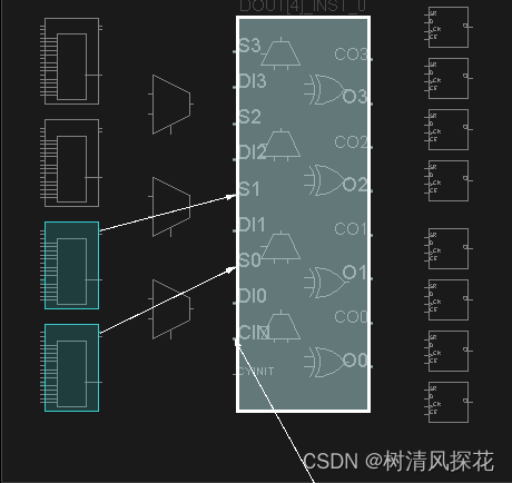
把2位加法扩展到6位加法,使用了进位链资源CARRY4(由选择器和异或门组成)。
2 逻辑门实现加法
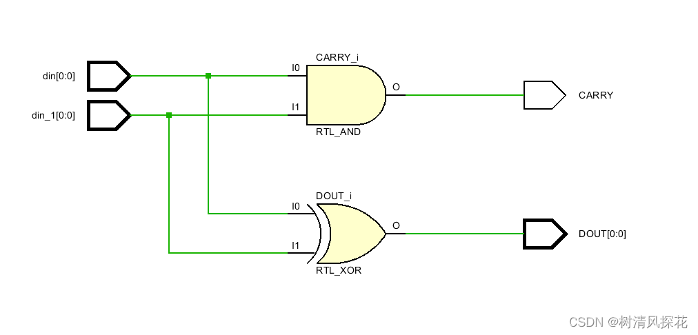
2.1 异或门和与门组成半加器
module half_add(
	input 		[0:0]				din,
	input 		[0:0]				din_1,
	output		[0:0]				DOUT,
	output							CARRY,


);
	assign  DOUT=din ^ din_1;
	assign  CARRY = din & din_1;

endmodule
2.1 RTL 原理图
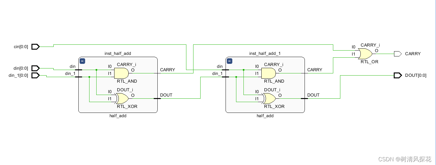
2.2 流水线全加器
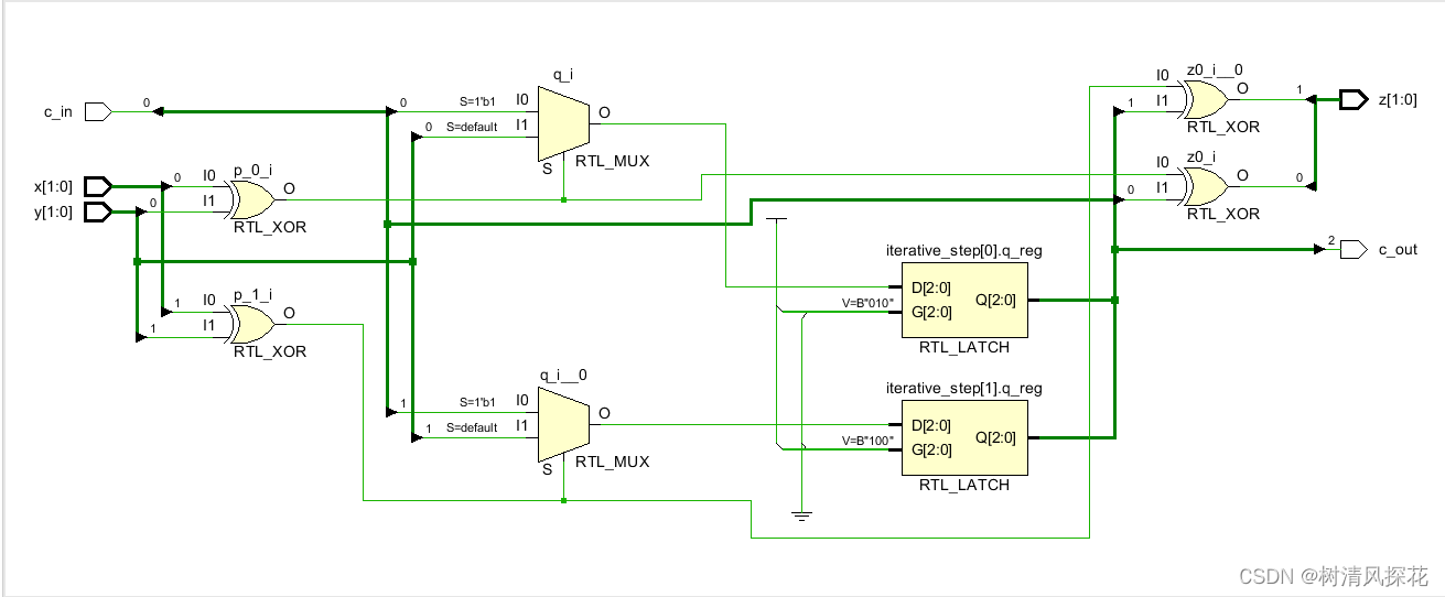
2.3 超前进位加法器
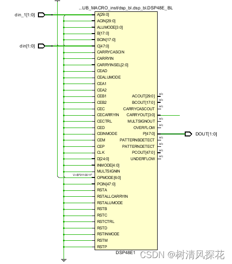
3 DSP实现加法


 1389
1389


 被折叠的 条评论
为什么被折叠?
被折叠的 条评论
为什么被折叠?
 到【灌水乐园】发言


