


一、原始代码
1\material material=GaN eg300=3.4 align=0.8 permitt=9.5 \
	mun=900 mup=10 vsatn=2e7 nc300=1.07e18 nv300=1.16e19 \
	real.index=2.67 imag.index=0.001 \
	taun0=$lt taup0=$lt
2\material material=AlGaN affinity=3.82 eg300=3.96 align=0.8 permitt=9.5 \
	mun=600 mup=10 nc300=2.07e18 nv300=1.16e19 \
	real.index=2.5 imag.index=0.001 \
	taun0=$lt taup0=$lt
3\mobility region=1 fmct.n fmct.p

4\method itlimit max.trap
5\method fermi compress
6\method newton trap maxtraps=10 climit=1e-4  ir.tol=1e-30 ix.tol=1e-30

7\material material=AlGaN affinity=3.82 eg300=3.96 align=0.8 permitt=9.5 \
	mun=600 mup=10 nc300=2.07e18 nv300=1.16e19 \
	real.index=2.5 imag.index=0.001 \
	taun0=$lt taup0=$lt

8\model print fermi fldmob srh pch.elec
二、各个部分参数的意义
1\material material=GaN eg300=3.4 align=0.8 permitt=9.5 \
	mun=900 mup=10 vsatn=2e7 nc300=1.07e18 nv300=1.16e19 \
	real.index=2.67 imag.index=0.001 \
	taun0=$lt taup0=$lt
#eg300:禁带宽度(300K) align:表示两种材料禁带宽度之差,有多大部分存在于导带。如语句:MATERIAL MATERIAL=InGaAs ALIGN=0.36 MATERIAL MATERIAL=InP align=0.36 材料InGaAs和材料InP的禁带宽度的差值有0.36存在于导带,有0.64存在于价带。permitt: 介电常数
#mun:低场电子迁移率  mup:低场空穴迁移率 vsatn:电子的饱和迁移速度 vsatp:空穴的饱和迁移速度  taurel.el 和 taurel.ho电子和空穴的弛豫时间  nc300:导带态密度(300k) nv300:价带态密度(300k)real.index和imag.index折射率的实部和虚部,可用来设置介电常数和吸收系数
taun0:SRH下电子复合寿命 taup0:SRH下空穴的复合寿命

2\material material=AlGaN affinity=3.82 eg300=3.96 align=0.8 permitt=9.5 \
	mun=600 mup=10 nc300=2.07e18 nv300=1.16e19 \
	real.index=2.5 imag.index=0.001 \
	taun0=$lt taup0=$lt
3\mobility region=1 fmct.n fmct.p  #fmct定义了电子和空穴的低场迁移率模型

4\method itlimit max.trap #itlimit表示最大计算次数,maxtraps表示最大的迭代次数,如果超过了最大计算次数会迭代(迭代的意思就是将偏压值减小一半)
fmct #低场迁移率模型的一种,表征温度和组分相关的迁移率模型,全称是(Farahmand Modified Caughey Thomas)
5\method fermi compress #athena中默认的氧化模型

6\method newton trap maxtraps=10 climit=1e-4  ir.tol=1e-30 ix.tol=1e-30#ir.tol:相对电流收敛准则,ix.tol:绝对电流收敛准则。

7\material material=AlGaN affinity=3.82 eg300=3.96 align=0.8 permitt=9.5 \
	mun=600 mup=10 nc300=2.07e18 nv300=1.16e19 \
	real.index=2.5 imag.index=0.001 \
	taun0=$lt taup0=$lt
#sffinity:电子亲和能
8\model print fermi fldmob srh pch.elec #pch.elec:指明在绝缘子或外部域的接口上存在极化电荷
二、光生成和复合过程模拟(来源于唐龙谷老师书籍的145页)
对于这一段材料定义语句进行详细分析,可以省去大量的查找资料的时间,也可以当作我自己的学习笔记进行复习使用。
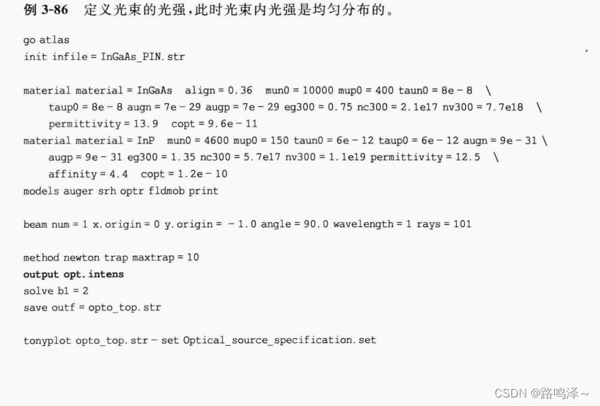
go atlas
init infile=InGaAs_PIN.str
material material=InGaAs align=0.6 mun0=10000 mup0=400 taun0=8e-8 \
taup0=8e-8 augn=7e-29 augp=7e-29 eg300=0.75 nc300=2.1e17 nv300=7.7e18 \
permittivity=13.9 copt=9.6e-11
#material=InGaAs:选定材料InGaAs,进行材料参数的设计。
#align=0.36:与InP材料禁带宽度之差的60%分布在导带上,换言之导带差占禁带宽度差的60%。
#mun0=10000 munp=400:低场电子迁移率为10000,低场空穴迁移率为400。
#taun0=8e-8 taunp0=8e-8:间接复合(SRH)下电子的寿命为8e-8,空穴的寿命为8e-8.
#augn=7e-29 augp=7e-29:augn和augp是与俄歇复合相关的两个参数
#eg300=0.75:300K下InGaAs材料的禁带宽度为0.75eV
#nc300=2.1e17 nv300=7.7e18:300k下InGaAs材料的导带态密度为2.1e17,价带态密度为7.7e18
#permittivity:介电常数13.9
#copt=9.6e-11:捕获速率为9.6e-11;同理有eopt为材料的激发参数
material material=InP mun0=4600 mup0=150 taun6e-12 taup0=6e-12 augn=9e-31 \
augp=9e-31 eg300=1.35 nc300=5.7e17 nv300=1.1e19 perimittivity=12.5 \
affinity=4.4 copt=1.2e-10
#affinity:电子亲和能,当材料定义中使用了align时使用affinity使导带之差满足align设置的比例。
models auger srh optr fldmob print
#optr:考虑导带电子和价带空穴直接复合并且发射光子的情形。
beam num=1 x.origin=0 y.origin=-1.0 angle=90 wavelength=1 rays=101
#光线的发射坐标为(0,-1.0),光线方向与x轴正方向夹角90,波长1微米,光线条数101条
method newton trap maxtrap=10
output opt.intense
#再输出文件中增加光强分布的信息
solve b1=2
save outf=opto_top.str
#定义光强为2W/cm2。
tonyplot opto_top.str-set Optical_source_specification.set
三、Devedit生成器中的语法规则和语句含义
文件来自silvaco-example-hemtex05.in
# (c) Silvaco Inc., 2018
go devedit
DevEdit version="2.1" library="1.15"

work.area left=0 top=-0.01 right=4.5 bottom=0.5

# SILVACO Library V1.15

region reg=1 mat=GaAs color=0xffb2 pattern=0x9 \
	points="0,0 1,0 1.1,0 1.5,0.05 0,0.05 0,0"
#
impurity id=1 region.id=1 imp=Donors color=0x906000 \
	x1=0 x2=0 y1=0 y2=0 \
	peak.value=2e+18 ref.value=1000000000000 comb.func=Multiply \
	rolloff.y=both conc.func.y=Constant \
	rolloff.x=both conc.func.x=Constant
#
constr.mesh region=1 default

region reg=2 mat=GaAs color=0xffb2 pattern=0x9 \
	points="2.9,0 3.5,0 4.5,0 4.5,0.05 2.5,0.05 2.9,0"
#
impurity id=1 region.id=2 imp=Donors color=0x906000 \
	x1=0 x2=0 y1=0 y2=0 \
	peak.value=2e+18 ref.value=1000000000000 comb.func=Multiply \
	rolloff.y=both conc.func.y=Constant \
	rolloff.x=both conc.func.x=Constant
#
constr.mesh region=2 default

region reg=3 mat=AlGaAs color=0xffff96 pattern=0x9 \
	points="4.5,0.05 4.5,0.08 0,0.08 0,0.05 1.5,0.05 1.75,0.05 2.25,0.05 2.5,0.05 4.5,0.05"
#
impurity id=1 region.id=3 imp="Composition Fraction X" color=0x906000 \#这里面impurity表示的是AlGaAs中Al的组分。
	x1=0 x2=0 y1=0 y2=0 \
	peak.value=0.22 ref.value=0 comb.func=Multiply \#peak.value=0.22 ref.value指Al的组分始终为0.22.
	rolloff.y=both conc.func.y=Constant \
	rolloff.x=both conc.func.x=Constant
#
impurity id=2 region.id=3 imp=Donors color=0x906000 \
	x1=0 x2=0 y1=0 y2=0 \
	peak.value=5e+15 ref.value=1000000000000 comb.func=Multiply \
	rolloff.y=both conc.func.y=Constant \
	rolloff.x=both conc.func.x=Constant
#
constr.mesh region=3 default

region reg=4 name=delta mat=AlGaAs color=0xffff96 pattern=0x9 \
	points="4.5,0.08 4.5,0.081 0,0.081 0,0.08 4.5,0.08"
#
impurity id=1 region.id=4 imp="Composition Fraction X" color=0x906000 \
	x1=0 x2=0 y1=0 y2=0 \
	peak.value=0.22 ref.value=0 comb.func=Multiply \
	rolloff.y=both conc.func.y=Constant \
	rolloff.x=both conc.func.x=Constant
#
impurity id=2 region.id=4 imp=Donors color=0x906000 \
	x1=0 x2=0 y1=0 y2=0 \
	peak.value=8e+18 ref.value=1000000000000 comb.func=Multiply \
	rolloff.y=both conc.func.y=Constant \
	rolloff.x=both conc.func.x=Constant
#
constr.mesh region=4 default

region reg=5 name=spacer mat=AlGaAs color=0xffff96 pattern=0x9 \
	points="0,0.081 4.5,0.081 4.5,0.084 0,0.084 0,0.081"
#
impurity id=1 region.id=5 imp="Composition Fraction X" color=0x906000 \
	x1=0 x2=0 y1=0 y2=0 \
	peak.value=0.22 ref.value=0 comb.func=Multiply \
	rolloff.y=both conc.func.y=Constant \
	rolloff.x=both conc.func.x=Constant
#
impurity id=2 region.id=5 imp=Donors color=0x906000 \
	x1=0 x2=0 y1=0 y2=0 \
	peak.value=5e+15 ref.value=1000000000000 comb.func=Multiply \
	rolloff.y=both conc.func.y=Constant \
	rolloff.x=both conc.func.x=Constant
#
constr.mesh region=5 default

region reg=6 mat=InGaAs color=0xffc8c8 pattern=0xa \
	points="0,0.084 4.5,0.084 4.5,0.098 0,0.098 0,0.084"
#
impurity id=1 region.id=6 imp="Composition Fraction X" color=0x906000 \
	x1=0 x2=0 y1=0 y2=0 \
	peak.value=0.78 ref.value=0 comb.func=Multiply \
	rolloff.y=both conc.func.y=Constant \
	rolloff.x=both conc.func.x=Constant
#
impurity id=2 region.id=6 imp=Donors color=0x906000 \
	x1=0 x2=0 y1=0 y2=0 \
	peak.value=5e+15 ref.value=1000000000000 comb.func=Multiply \
	rolloff.y=both conc.func.y=Constant \
	rolloff.x=both conc.func.x=Constant
#
constr.mesh region=6 default

region reg=7 mat=AlGaAs color=0xffff96 pattern=0x9 \
	points="0,0.098 4.5,0.098 4.5,0.101 0,0.101 0,0.098"
#
impurity id=1 region.id=7 imp=Acceptors color=0x906000 \
	x1=0 x2=0 y1=0 y2=0 \
	peak.value=150000000000000 ref.value=1000000000000 comb.func=Multiply \
	rolloff.y=both conc.func.y=Constant \
	rolloff.x=both conc.func.x=Constant
#
impurity id=2 region.id=7 imp="Composition Fraction X" color=0x906000 \
	x1=0 x2=0 y1=0 y2=0 \
	peak.value=0.22 ref.value=0 comb.func=Multiply \
	rolloff.y=both conc.func.y=Constant \
	rolloff.x=both conc.func.x=Constant
#
constr.mesh region=7 default

region reg=8 mat=AlGaAs color=0xffff96 pattern=0x9 \
	points="0,0.101 4.5,0.101 4.5,0.102 0,0.102 0,0.101"
#
impurity id=1 region.id=8 imp="Composition Fraction X" color=0x906000 \
	x1=0 x2=0 y1=0 y2=0 \
	peak.value=0.22 ref.value=0 comb.func=Multiply \
	rolloff.y=both conc.func.y=Constant \
	rolloff.x=both conc.func.x=Constant
#
impurity id=2 region.id=8 imp=Donors color=0x906000 \
	x1=0 x2=0 y1=0 y2=0 \
	peak.value=2e+18 ref.value=1000000000000 comb.func=Multiply \
	rolloff.y=both conc.func.y=Constant \
	rolloff.x=both conc.func.x=Constant
#
constr.mesh region=8 default

region reg=9 mat=AlGaAs color=0xffff96 pattern=0x9 \
	points="0,0.102 4.5,0.102 4.5,0.14 0,0.14 0,0.102"
#
impurity id=1 region.id=9 imp=Acceptors color=0x906000 \
	x1=0 x2=0 y1=0 y2=0 \
	peak.value=100000000000000 ref.value=1000000000000 comb.func=Multiply \
	rolloff.y=both conc.func.y=Constant \
	rolloff.x=both conc.func.x=Constant
#
impurity id=2 region.id=9 imp="Composition Fraction X" color=0x906000 \
	x1=0 x2=0 y1=0 y2=0 \
	peak.value=0.22 ref.value=0 comb.func=Multiply \
	rolloff.y=both conc.func.y=Constant \
	rolloff.x=both conc.func.x=Constant
#
constr.mesh region=9 default

region reg=10 name=GaAs mat=AlGaAs color=0xffb2 pattern=0x9 \
	points="0,0.14 4.5,0.14 4.5,0.5 0,0.5 0,0.14"
#
impurity id=1 region.id=10 imp=Acceptors color=0x906000 \
	x1=0 x2=0 y1=0 y2=0 \
	peak.value=100000000000000 ref.value=1000000000000 comb.func=Multiply \
	rolloff.y=both conc.func.y=Constant \
	rolloff.x=both conc.func.x=Constant
#
constr.mesh region=10 default

region reg=11 name=source mat=Gold elec.id=1 work.func=0 color=0xe5ff pattern=0xb \
	points="0,0 0,-0.01 1,-0.01 1,0 0,0"
#
constr.mesh region=11 default

region reg=12 name=drain mat=Gold elec.id=2 work.func=0 color=0xe5ff pattern=0xb \
	points="3.5,0 3.5,-0.01 4.5,-0.01 4.5,0 3.5,0"
#
constr.mesh region=12 default

region reg=13 name=gate mat=Gold elec.id=3 work.func=0 color=0xe5ff pattern=0xb \
	points="1.75,0.05 1.75,0 2.25,0 2.25,0.05 1.75,0.05"
#
constr.mesh region=13 default


impurity id=1 imp=Donors color=0x906000 \
	x1=0 x2=1 y1=0 y2=0.08 \
	peak.value=5e+21 ref.value=1e+20 comb.func=Multiply \
	rolloff.y=both conc.func.y="Gaussian (Dist)" conc.param.y=0.048 \
	rolloff.x=both conc.func.x="Error Function" conc.param.x=0.02
impurity id=2 imp=Donors color=0x906000 \
	x1=3.5 x2=4.5 y1=0 y2=0.08 \
	peak.value=5e+21 ref.value=1e+20 comb.func=Multiply \
	rolloff.y=both conc.func.y="Gaussian (Dist)" conc.param.y=0.048 \
	rolloff.x=both conc.func.x="Error Function" conc.param.x=0.02

# Set Meshing Parameters
#
base.mesh height=0.1 width=0.25
#
bound.cond !apply max.slope=28 max.ratio=300 rnd.unit=5e-05 line.straightening=1 align.points when=automatic
#
imp.refine min.spacing=0.02
#
constr.mesh max.angle=90 max.ratio=3000 max.height=1 \
	max.width=1 min.height=0.0001 min.width=0.0001
#
constr.mesh type=Semiconductor default
#
constr.mesh type=Insulator default
#
constr.mesh type=Metal default
#
constr.mesh type=Other default
#
constr.mesh region=1 default
#
constr.mesh region=2 default
#
constr.mesh region=3 default
#
constr.mesh region=4 default
#
constr.mesh region=5 default
#
constr.mesh region=6 default
#
constr.mesh region=7 default
#
constr.mesh region=8 default
#
constr.mesh region=9 default
#
constr.mesh region=10 default
#
constr.mesh region=11 default
#
constr.mesh region=12 default
#
constr.mesh region=13 default
#
# Perform mesh operations
#
Mesh Mode=MeshBuild
refine mode=y x1=0.068 y1=0.0123 x2=1.48 y2=0.038
refine mode=y x1=2.492 y1=0.0106 x2=4.402 y2=0.044
refine mode=y x1=0.106 y1=0.0089 x2=1.511 y2=0.0414
refine mode=y x1=2.515 y1=0.0046 x2=4.357 y2=0.0405
refine mode=x x1=1.571 y1=0.0568 x2=2.417 y2=0.334
refine mode=x x1=0.084 y1=0.0063 x2=0.891 y2=0.3477
refine mode=x x1=3.602 y1=0.0055 x2=4.41 y2=0.3383
refine mode=y x1=0.038 y1=0.0414 x2=1.563 y2=0.0457
refine mode=y x1=2.454 y1=0.0397 x2=4.448 y2=0.044
refine mode=y x1=0.076 y1=0.0551 x2=4.455 y2=0.2887
refine mode=y x1=0.031 y1=0.0524 x2=4.425 y2=0.074
refine mode=y x1=0.068 y1=0.0516 x2=4.44 y2=0.0761
refine mode=y x1=0.023 y1=0.0768 x2=4.463 y2=0.0787
refine mode=y x1=0.084 y1=0.106 x2=4.47 y2=0.1829
refine mode=y x1=0.061 y1=0.1044 x2=4.47 y2=0.1344
refine mode=y x1=0.046 y1=0.1036 x2=4.433 y2=0.1053
refine mode=y x1=0.061 y1=0.0862 x2=4.433 y2=0.0966
refine mode=y x1=0.038 y1=0.0856 x2=4.433 y2=0.0961
refine mode=x x1=1.556 y1=0.0499 x2=2.462 y2=0.2322

imp.refine min.spacing=0.02

constr.mesh max.angle=90 max.ratio=3000 max.height=1 \
	max.width=1 min.height=0.0001 min.width=0.0001
#
constr.mesh type=Semiconductor default
#
constr.mesh type=Insulator default
#
constr.mesh type=Metal default
#
constr.mesh type=Other default


base.mesh height=0.1 width=0.25

bound.cond !apply max.slope=28 max.ratio=300 rnd.unit=5e-05 line.straightening=1 align.Points when=automatic


structure outf=hemtex05_0.str


go atlas

title  GaAs-AlGaAs-InGaAs Pseudomorphic HEMT simulation

# Load the structure generated in DEVEDIT...
# While running in the deckbuild after DEVEDIT input deck the structure is
# transfered automatically: no mesh statement is needed, comment it out

#mesh infile=hemtex05_0.str master.in


# Define the workfunction for the gate contact

contact     name=gate   workfunction=4.55

# Define material parameters on material-by-material basis

material material=GaAs   align=0.6
material material=AlGaAs align=0.6
material material=InGaAs align=0.6 mun0=12000 mup0=2000 vsat=2.e7 \
                         taun0=1.e-8 taup0=1.e-8

# Define physical models on material-by material basis

models material=GaAs   consrh conmob fldmob evsatmod=0 print
models material=AlGaAs consrh conmob fldmob evsatmod=0 print
models material=InGaAs srh           fldmob evsatmod=0 print

# Initial solution

solve    init
save outf=hemtex05_1.str
tonyplot  hemtex05_1.str -set hemtex05_1.set


# Include bands potential, and current flowlines into output

output con.band val.band flowlines


# Apply a set of biases at the gate and save solutions

solve vgate= 0    outf=hemtex05_A_0.bin
solve vgate=-0.2  outf=hemtex05_Ag-02.bin
solve vgate=-0.4  outf=hemtex05_Ag-04.bin

# Calculate ID-VD characteristic at zero gate bias

load inf=hemtex05_A_0.bin

log outf=hemtex05_1.log


solve outf=hemtex05_A_0.str master
solve vdrain=0.02
solve vdrain=0.05
solve vdrain=0.1 vstep=0.1 vfinal=2.0 name=drain
save outf=hemtex05_Ad2.str master

# Calculate ID-VD characteristic at VG=-0.2

load inf=hemtex05_Ag-02.bin
log outf=hemtex05_2.log

solve prev
solve vdrain=0.02
solve vdrain=0.05
solve vdrain=0.1 vstep=0.1 vfinal=2.0 name=drain
save outf=hemtex05_Ad2g-02.str master

# Calculate ID-VD characteristic at VG=-0.4

load inf=hemtex05_Ag-04.bin
log outf=hemtex05_3.log

solve prev
solve vdrain=0.02
solve vdrain=0.05
method   itlimit=10 trap atrap=0.5 maxtrap=8
solve vdrain=0.1 vstep=0.1 vfinal=2.0 name=drain
save outf=hemtex05_Ad2g-04.str master


# Calculate ID-VG characteristics at VD=2.0 V
# Simultaneously apply small signal perturbation to get AC parameters

load inf=hemtex05_Ad2.str master

log outf=hemtex05_4.log master

solve vgate=0 vstep=-0.1 vfinal=-1.5 name=gate ac freq=1e6
save outf=hemtex05_Ad2g_15.str master


extract init inf="hemtex05_4.log"

extract name="Vt" (xintercept(maxslope(curve(v."gate",i."drain"))))

# Maximum saturation current
extract name="Idss" max(i."drain")

# Gate voltage Vg@Idss*0.3 at Id=0.3Idss
extract name="Vgs@0.3Idss" x.val from curve (v."gate", i."drain") where y.val=$"Idss"*0.3

# Maximum gate-source capacitance
extract name="Cgs_max" max(abs(c."gate""source"))

# Gate-source capacitance at Vg=0
extract name="Cgs_Vgs0" y.val from curve (v."gate", abs(c."gate""source")) where x.val=0.0

# Gate-source capacitance at Id=0.3Idss
extract name="Cgs_Vgs@0.3Idss" y.val from curve (v."gate", abs(c."gate""source")) where x.val=$"Vgs@0.3Idss"

# Maximum transconductance
extract name="Gm_max" max(abs(g."drain""gate"))

# Transconductance at Vg=0
extract name="Gm_Vgs0" y.val from curve (v."gate", abs(g."drain""gate")) where x.val=0.0

# Transconductance at Id=0.3Idss
extract name="Gm_Vgs@0.3Idss" y.val from curve (v."gate", abs(g."drain""gate")) where x.val=$"Vgs@0.3Idss"
# Displaying the results

# Plot ID-VD characteristics

tonyplot -overlay hemtex05_1.log hemtex05_2.log hemtex05_3.log -set hemtex05_log.set


# Plot ID-VG characteristic
tonyplot hemtex05_4.log -set hemtex05_log1.set

quit


 3566
3566


 被折叠的 条评论
为什么被折叠?
被折叠的 条评论
为什么被折叠?
 到【灌水乐园】发言


