


 文章详细描述了一个半导体器件的建模过程,包括硅片掺杂、扩散、电极定义、电子浓度计算以及光照对电子浓度的影响。重点展示了CCDX01实例中的源代码和各个步骤的解释。
来自于ccdx01.in仿真例子。
一、(1)源代码
# (c) Silvaco Inc., 2018
go athena
line x loc= 0.00 spac=0.5
line x loc= 3.00 spac=0.1
line x loc= 3.20 spac=0.1
line x loc= 4.70 spac=0.25
line x loc= 6.20 spac=0.1
line x loc= 7.00 spac=0.2
line y loc=0.00 spac=0.05
line y loc=0.6 spac=0.1
line y loc=3.0 spac=0.5
# Define material, orientation, initial doping
init silicon c.boron=5e15 orientation=100 space.mult=2
# form n- active layer at surface
implant phosphorus dose=8e11 energy=120
# active layer diffusion
diffuse time=60 temp=950 nitro
# Deposit gate oxide
deposit oxide thick=0.04 divisions=3
# mask for the p- implant under transfer gate
deposit photo thick=3.0 divisions=2
etch photores start x=7 y=-10.0
etch cont x=7 y=10.0
etch cont x=3.5 y=10.0
etch done x=3.5 y=-10.0
relax y.min=1.0
# Implant p- region
implant boron dose=1e11 energy=80
etch photores all
#drive diffusion : commented out for speed
#method fermi compress
#diffus time=220 temp=1000 nitro press=1.00
deposit poly thick=0.12 div=1
etch poly start x=3.0 y=-5
etch cont x=3.0 y=5
etch cont x=3.2 y=5
etch done x=3.2 y=-5
etch poly start x=6.2 y=-5
etch cont x=6.2 y=5
etch cont x=7.0 y=5
etch done x=7.0 y=-5
deposit photo thick=1.0 divisions=8
etch photo right p1.x=6.2
etch oxide right p1.x=6.2
# Implant n+ drain region
implant arsenic dose=1e15 energy=50
strip
#drain anneal : commented out for speed
#method fermi compress
#diffus time=30 temp=900 nitro press=1.00
deposit alum thick=0.1 div=2
etch alum left p1.x=6.5
electrode name=sto_gate x=0
electrode name=tra_gate x=4
electrode name=drain x=6.9
electrode name=substrate backside
# extract process parameters
# here active layer/substrate junction is SECOND from the surface
extract name="storage_xj" xj material="Silicon" mat.occno=1 x.val=1 junc.occno=2
extract name="transfer_xj" xj material="Silicon" mat.occno=1 x.val=5 junc.occno=2
structure outf=ccdex01_0.str
tonyplot ccdex01_0.str -set ccdex01_0.set
go atlas
contact name=sto_gate n.poly
contact name=tra_gate n.poly
material taun0=1e-7 taup0=1e-7
models cvt consrh bgn auger print
interface qf=3e10
beam num=1 wavelength=0.6 x.ori=0 y.ori=-1 max.win=2 angle=90
solve init
method newton climit=1e-4
solve v1=-6 v2=-6
solve vdrain=0.1
solve vdrain=1 vstep=1 vfinal=15 name=drain
#save empty structure
save outf=ccdex01_1.str
tonyplot ccdex01_1.str -set ccdex01_1.set
#extract electron concentration in empty well (1.0e4 is to scale into I/cm^3)
extract init inf="ccdex01_1.str"
extract name="n_in_empty_well" 1.0e+4*area from curve(depth,n.conc material="Silicon" mat.occno=1 x.val=1.0)
# now turn on light beam in transient
solve b1=1 ramp.lit ramptime=5e-9 dt=1e-11 tstop=20e-9 outf=light.str master onefile
solve b1=0 ramp.lit ramptime=5e-9 dt=1e-10 tstop=50e-9
#save charged structure
save outf=ccdex01_2.str
tonyplot ccdex01_2.str -set ccdex01_2.set
#extract electron concentration in full well (1.0e4 is to scale into I/cm^3)
extract init inf="ccdex01_2.str"
extract name="n_in_full_well" 1.0e+4*area from curve(depth,n.conc material="Silicon" mat.occno=1 x.val=1.0)
extract name="stored_n" $n_in_full_well - $n_in_empty_well
# now do transfer
# ramp transfer gate to +2V
log outf=transfer.log
solve v2=2 ramptime=1e-9 dt=1e-11 tstop=1e-6 outf=ccdex01_00 master
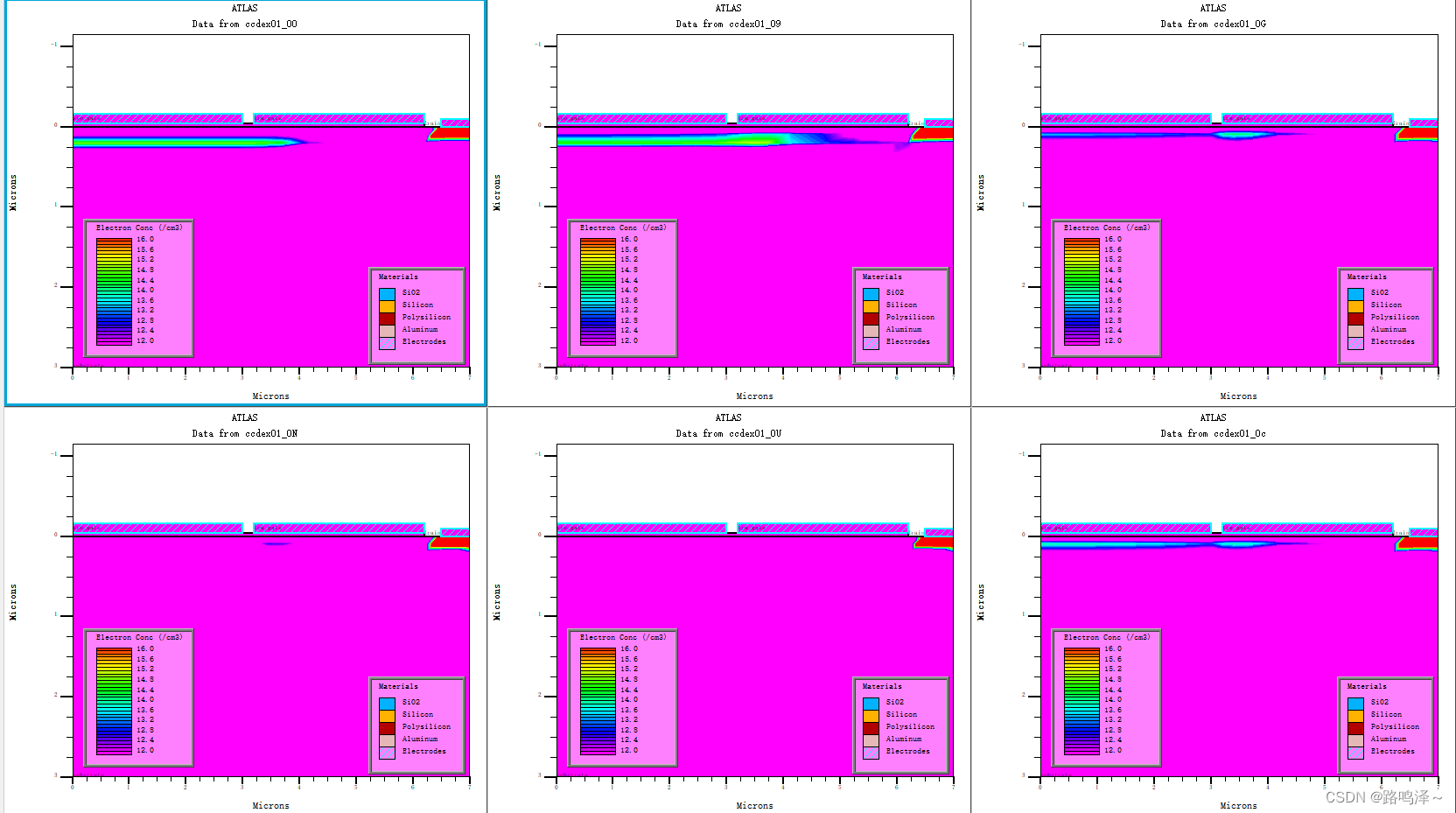
tonyplot ccdex01_00 ccdex01_09 ccdex01_0G ccdex01_0N ccdex01_0U ccdex01_0c -set ccdex01_3.set
quit
(2)各部分的解释:
# (c) Silvaco Inc., 2018
go athena

line x loc= 0.00 spac=0.5
line x loc= 3.00 spac=0.1
line x loc= 3.20 spac=0.1
line x loc= 4.70 spac=0.25
line x loc= 6.20 spac=0.1
line x loc= 7.00 spac=0.2

line y loc=0.00  spac=0.05
line y loc=0.6   spac=0.1
line y loc=3.0   spac=0.5


# Define material, orientation, initial doping
init silicon c.boron=5e15 orientation=100 space.mult=2

# form n- active layer at surface
implant phosphorus dose=8e11 energy=120

# active layer diffusion
diffuse time=60 temp=950 nitro

# Deposit gate oxide

deposit oxide thick=0.04 divisions=3


# mask for the p- implant under transfer gate
deposit photo thick=3.0 divisions=2

etch photores start x=7 y=-10.0
etch cont x=7 y=10.0
etch cont x=3.5 y=10.0
etch done x=3.5 y=-10.0


relax y.min=1.0


# Implant p- region
implant boron dose=1e11 energy=80

etch photores all

#drive diffusion : commented out for speed
#method fermi compress
#diffus time=220 temp=1000 nitro press=1.00

deposit poly thick=0.12 div=1

etch poly start x=3.0 y=-5
etch cont x=3.0 y=5
etch cont x=3.2 y=5
etch done x=3.2 y=-5

etch poly start x=6.2 y=-5
etch cont x=6.2 y=5
etch cont x=7.0 y=5
etch done x=7.0 y=-5

deposit photo thick=1.0 divisions=8

etch photo right p1.x=6.2
etch oxide right p1.x=6.2

# Implant n+ drain region
implant arsenic dose=1e15 energy=50

strip

#drain anneal : commented out for speed
#method fermi compress
#diffus time=30 temp=900 nitro press=1.00

deposit alum thick=0.1 div=2
etch alum left p1.x=6.5

electrode name=sto_gate x=0 #store,该栅极用来存储电荷
electrode name=tra_gate x=4 #transfer,该栅极用来输运电荷
electrode name=drain x=6.9
electrode name=substrate backside

# extract process parameters
# here active layer/substrate junction is SECOND from the surface
extract name="storage_xj" xj material="Silicon" mat.occno=1 x.val=1 junc.occno=2
extract name="transfer_xj" xj material="Silicon" mat.occno=1 x.val=5 junc.occno=2   提取的位置和结出现的次数


structure outf=ccdex01_0.str
tonyplot ccdex01_0.str -set ccdex01_0.set


go atlas

contact name=sto_gate n.poly
contact name=tra_gate n.poly

material taun0=1e-7 taup0=1e-7 电子和空穴的寿命
models cvt consrh bgn auger print
interface qf=3e10

beam num=1 wavelength=0.6 x.ori=0 y.ori=-1 max.win=2 angle=90
solve init

method newton climit=1e-4

solve v1=-6 v2=-6 #V1是stro_gate;V2是tra_gate
solve vdrain=0.1
solve vdrain=1 vstep=1 vfinal=15 name=drain

#save empty structure
save outf=ccdex01_1.str
tonyplot  ccdex01_1.str -set ccdex01_1.set


#extract electron concentration in empty well (1.0e4 is to scale into I/cm^3)
extract init inf="ccdex01_1.str"  #导入提取的数据来源文件
extract name="n_in_empty_well" 1.0e+4*area from curve(depth,n.conc material="Silicon" mat.occno=1 x.val=1.0)
#提取位于x=1位置,Si材料中,曲线围的面积(电子浓度和深度的曲线)再乘以1e4,得到了电子的浓度。

# now turn on light beam in transient

solve b1=1 ramp.lit ramptime=5e-9 dt=1e-11 tstop=20e-9 outf=light.str master onefile
# SOLVE .... OUTFILE=<filename>.sta MASTER 产生一系列的文件,但是在语句的最后加上onefile,后一点的数据就会覆盖前一点的数据,保存在light.str中,所以到最后得到的light.str仅仅保存了一个点的数据。
solve b1=0 ramp.lit ramptime=5e-9 dt=1e-10 tstop=50e-9

#save charged structure
save outf=ccdex01_2.str
tonyplot  ccdex01_2.str -set ccdex01_2.set


#extract electron concentration in full well (1.0e4 is to scale into I/cm^3)
extract init inf="ccdex01_2.str"
extract name="n_in_full_well" 1.0e+4*area from curve(depth,n.conc material="Silicon" mat.occno=1 x.val=1.0)
extract name="stored_n" $n_in_full_well - $n_in_empty_well


# now do transfer
# ramp transfer gate to +2V
log outf=transfer.log
solve v2=2 ramptime=1e-9 dt=1e-11 tstop=1e-6 outf=ccdex01_00 master
# (1) SAVE OUTFILE=<filename> (2) SOLVE .... OUTFILE=<filename>.sta MASTER 用于产生文件存在上述两种方式,当使用第二种方式进行存储时,在这种情况下,在求解语句中解决的每个偏差点都将保存一个结构文件。文件名的最后一个字母将自动按字母顺序递增: (i.e., *.sta,*.stb, *.stc..., and so on);在本语句中产生的文件为(ccdex01_00, ccdex01_01, ccdex01_02, ccdex01_03...,and so on)

tonyplot ccdex01_00 ccdex01_09 ccdex01_0G ccdex01_0N ccdex01_0U ccdex01_0c -set ccdex01_3.set
#由上述可知储存的文件为ccdex01_00, ccdex01_01, ccdex01_02,...ccdex01_09,ccdex01_0A,ccdex01_0B,...ccdex01_0Z,ccdex01_0a,ccdex01_0b,ccdex01_0c,...ccdex01_0z)产生的文件排序为0,1,2,3,4,5,6,7,8,9,A,B,...X,Y,Z,a,,b,c,...x,y,z,10,11,12,13,14.

quit
对于施加光照的角度问题Atlas手册1119页上有图,容易观察到angle=90时光线是垂直于器件入射的,当angle=270时光线从背面垂直于器件入射;max.window和min.window为光线右侧和左侧的开口宽度。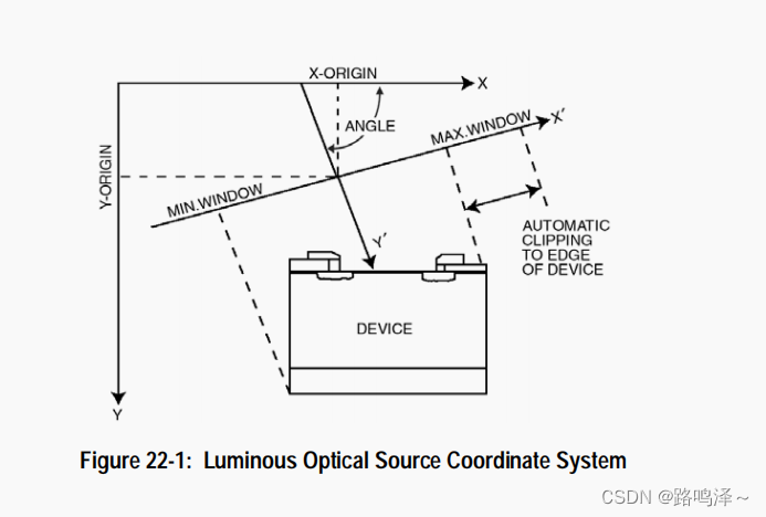
二、当stro_gate=-6 tra_gate=-6 vdrain=15时,ccd中的载流子浓度分布;
如图所示: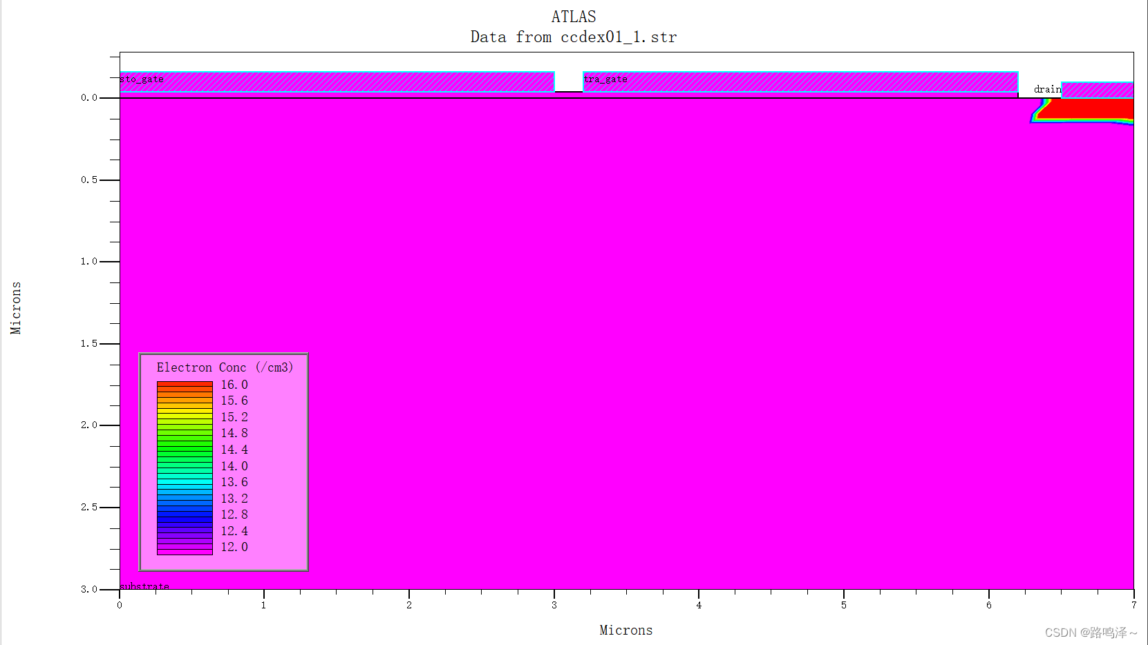
三、stro_gate=-6 tra_gate=-6 vdrain=15时,且施加光强为1W/cm-2,波长为600nm,垂直入射时,材料中电子的浓度。
如图所示: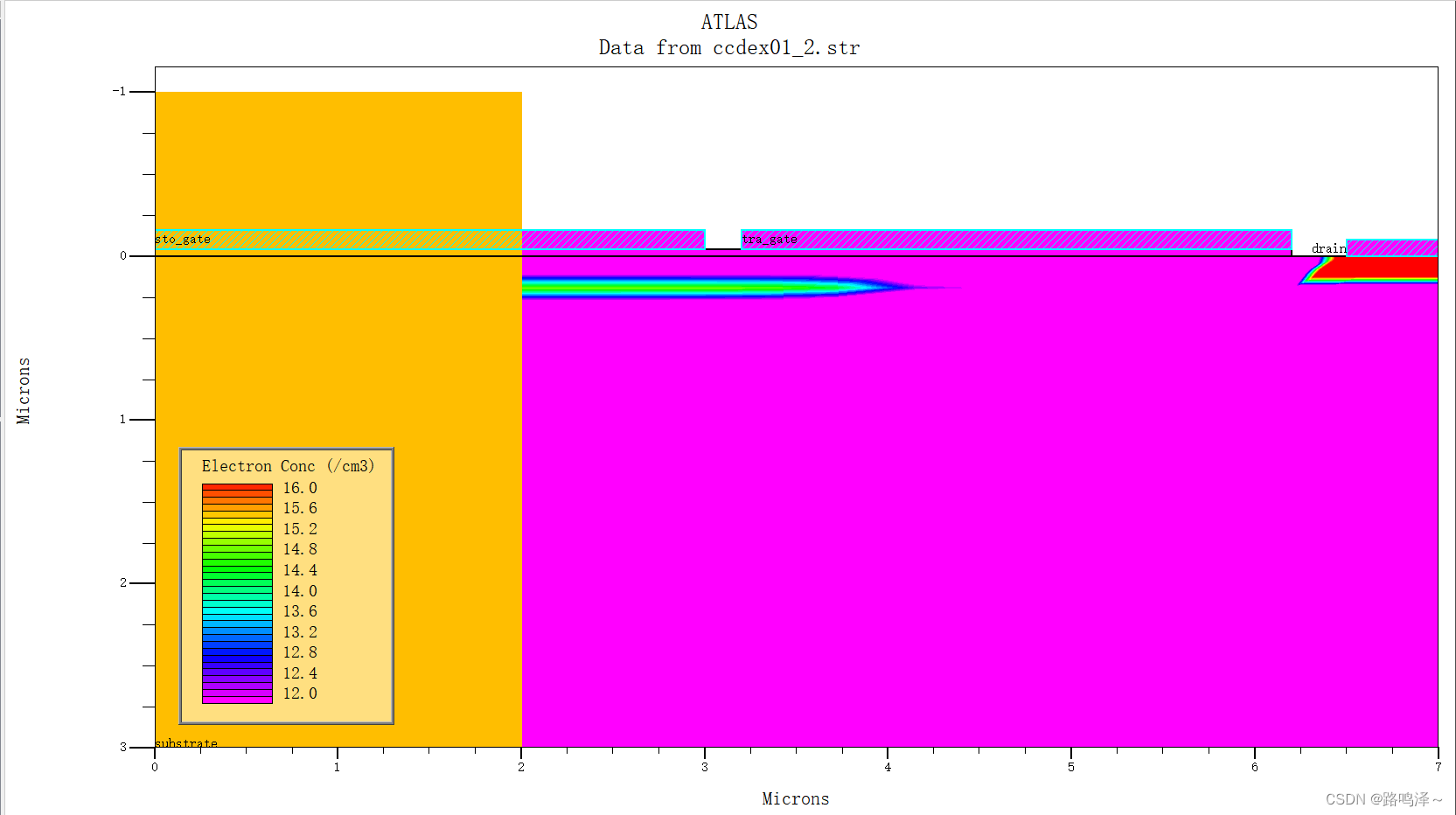
被光照图例遮住的x<2,的部分的电子的分布为: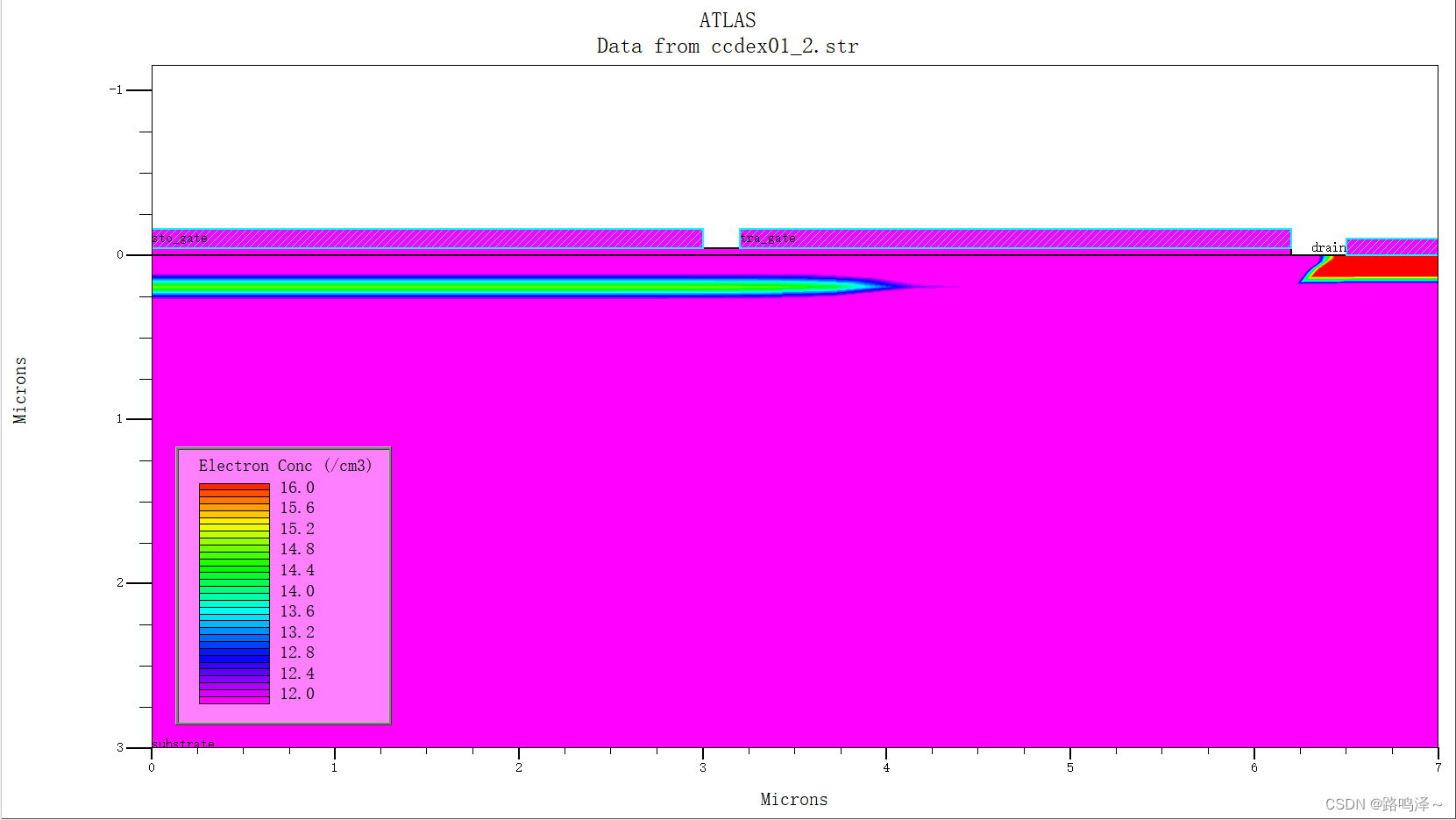
四、 产生文件ccdex01_00 ,ccdex01_09, ccdex01_0G ,ccdex01_0N ,ccdex01_0U ,ccdex01_0c的条件sto_gate=-6V,Vdrain=15V,tra_gate不断变化。
ccdex01_00,sto_gate=-6V,Vdrain=15V,tra_gate=-6
ccdex01_09,sto_gate=-6V,Vdrain=15V,tra_gate=-4.149
ccdex01_0G,sto_gate=-6V,Vdrain=15V,tra_gate=-0.872
ccdex01_0N,sto_gate=-6V,Vdrain=15V,tra_gate=0.68
ccdex01_0U,sto_gate=-6V,Vdrain=15V,tra_gate=2
ccdex01_0c,sto_gate=-6V,Vdrain=15V,tra_gate=2,但是ccdex_0U和ccdex_0c施加电压的时间是不同的。
电子浓度分布图如图所示:


 1万+
1万+

 被折叠的 条评论
为什么被折叠?
被折叠的 条评论
为什么被折叠?
 到【灌水乐园】发言


