


传统的测频法原理
直接计数单位时间内被测信号的脉冲数。


- 在理想条件下:
门控时间=基准时钟的整数倍,门控时间=待测信号的整数倍,计数器检测上升沿
对照示意图,可得如下公式(1)(2):
|
| (1) |
|
| (2) |
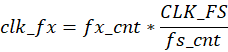
得到待测时钟
|
| (3) |
其中CLK_FS为基准时钟,clk_fx待测信号,GATE_TIME门控时间,
fs_cnt为单位时间内的基准时钟的个数,
fx_cnt单位时间内的待测时钟的个数。
-
实际条件下:
门控信号不等于待测信号的整数倍
在对待测信号的计数时会产生误差∆fx_cnt=±1
由公式(3)计算得到待测信号的误差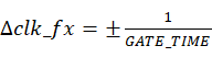 ,通过计算可以得到相对误差
 ,因此测量低频信号会产生较大误差.
等精度频率计原理
测量相对误差与被测信号的大小无关,实现整个频段的等精度测量

由图可以看出门控信号是待测信号的整数倍,这样对于基准信号计数时产生误差![]() ,从而使门控时间产生误差:
,从而使门控时间产生误差:![]() ,
,
最后被测时钟的误差: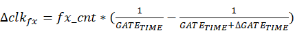 ,
,
相对误差: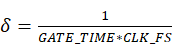 ,相对误差与被测信号,只与被测信号的大小无关。
实验程序设计
-
RTL视图
由以下四个模块:gate, pexg , CNT, seg_led。
模块gate的作用:通过待测信号生成周期是待测信号周期整数倍(5000)的闸门信号gate,以及一个与基准时钟同步的gate_fs信号。
模块pexg:捕获gate信号和gate_fs的下降沿。
模块CNT:用gate和gate_fs分别待测信号和基准时钟计数,得到fs_cnt和fx_cnt,并将计算待测信号的频率date_fx。
模块seg_led:用七段数码管显示测量值。

-
代码实现
顶层模块top_cymometer:
module top_cymometer(
    //system clock
    input                  sys_clk  ,    // 时钟信号
    input                  sys_rst_n,    // 复位信号
//spi没有使用
//		input  CS_N,
//		input  SCLK,
//		output MISO,
    //cymometer interface
    input                  clk_fx   ,    // 被测时钟
//    output                 clk_out  ,    // 输出时钟
	output [7:0] led0,
	output [7:0] led1,
	output [7:0] led2,
	output [7:0] led3,
	output [63:0]data_fx
);

//parameter define
parameter    CLK_FS = 26'd50000000;      // 基准时钟频率值


gate//生成门控信号
(
        .clk_fs      (sys_clk  ),     // 基准时钟信号
        .rst_n       (sys_rst_n),  // 复位信号

        //cymometer interface
        .clk_fx      (clk_fx   ), //待测信号
		  .gate(gate ) , //门控信号
		  .gate_fs(gate_fs) // 同步到基准时钟的门控信号
		  );

pexg//边沿捕获
(
        .clk_fs      (sys_clk  ),     // 基准时钟信号
        .rst_n       (sys_rst_n),  // 复位信号

		  .gate(gate ) , //门控信号
		  .gate_fs(gate_fs), // 同步到基准时钟的门控信号
       .clk_fx      (clk_fx), //待测信号

		  .neg_gate_fs(neg_gate_fs),
		  .neg_gate_fx(neg_gate_fx)
		  );

CNT
    (

	 //system clock
        .clk_fs      (sys_clk  ),     // 基准时钟信号
        .rst_n       (sys_rst_n),  // 复位信号

        //cymometer interface
        .clk_fx      (clk_fx   ), //待测信号
		  .gate(gate )  ,//门控信号
		  .gate_fs(gate_fs) ,// 同步到基准时钟的门控信号
		  .neg_gate_fs(neg_gate_fs),
		  .neg_gate_fx(neg_gate_fx),

		  .fs_cnt(fs_cnt)      ,          // 门控时间内基准时钟的计数值
		  .fx_cnt(fx_cnt)      ,           // 门控时间内被测时钟的计数值
        .data_fx_temp(data_fx)
);
//通过SPI模块实现与单片机通信
//spi(.clk(sys_clk),
//    .rst_n(sys_rst_n),
//    .CS_N(CS_N),
//    .SCLK(SCLK),
//    .MOSI(MOSI),
//    .txd_data(data_fx),
//    .MISO  (MISO)
//	 );
//实现比较,最后调试是通过signaltap分析
//seg_led u_seg_led(
//    //module clock
//    .clk         (sys_clk  ),            // 数码管驱动模块的驱动时钟
//    .rst_n       (sys_rst_n),            // 复位信号
   //user interface
//    .data        (data_fx  ),            // 被测频率值
//   .seg_led0	(led0),
//	.seg_led1	(led1),
//	.seg_led2	(led2),
//	.seg_led3 	(led3)
//);
endmodulegate模块:产生门控信号gate和同步到基准时钟下的门控信号gate_fs
module gate
(
        input                 clk_fs ,     // 基准时钟信号
        input                 rst_n   ,  // 复位信号

        //cymometer interface
        input                 clk_fx ,//待测信号
		  output		reg				gate , //门控信号
		  output    reg           gate_fs // 同步到基准时钟的门控信号
		  );

localparam   GATE_TIME = 16'd5_000;        // 门控时间设置
reg    [15:0]   gate_cnt    ;           // 门控计数

reg             gate_fs_r   ;           // 用于同步gate信号的寄存器

//门控信号计数器,使用被测时钟计数
always @(posedge clk_fx or negedge rst_n) begin
    if(!rst_n)
        gate_cnt <= 16'd0;
    else if(gate_cnt == GATE_TIME + 5'd20)
        gate_cnt <= 16'd0;
    else
        gate_cnt <= gate_cnt + 1'b1;
end


//门控信号,拉高时间为GATE_TIME个实测时钟周期
always @(posedge clk_fx or negedge rst_n) begin
    if(!rst_n)
        gate <= 1'b0;
    else if(gate_cnt < 4'd10)
        gate <= 1'b0;
    else if(gate_cnt < GATE_TIME + 4'd10)
        gate <= 1'b1;
    else if(gate_cnt <= GATE_TIME + 5'd20)
        gate <= 1'b0;
    else
        gate <= 1'b0;
end

//将门控信号同步到基准时钟下
always @(posedge clk_fs or negedge rst_n) begin
    if(!rst_n) begin
        gate_fs_r <= 1'b0;
        gate_fs   <= 1'b0;
    end
    else begin
        gate_fs_r <= gate;
        gate_fs   <= gate_fs_r;
    end
endpexg模块:边沿检测,得到的基准时钟下的gate的下降和待测时钟信号下gate的下降沿
module pexg
(
        input                 clk_fs ,     // 基准时钟信号
        input                 rst_n   ,  // 复位信号


        input                 clk_fx ,
			input gate,
			input gate_fs     ,
		  output    neg_gate_fs,
		  output    neg_gate_fx
		  );
reg                gate_fs_d0  ;           // 用于采集基准时钟下gate下降沿
reg                gate_fs_d1  ;           //
reg                gate_fx_d0  ;           // 用于采集被测时钟下gate下降沿
reg                gate_fx_d1  ;           //
//wire define

//边沿检测,捕获信号下降沿
assign neg_gate_fs = gate_fs_d1 & (~gate_fs_d0);
assign neg_gate_fx = gate_fx_d1 & (~gate_fx_d0);


//打拍采门控信号的下降沿(被测时钟)
always @(posedge clk_fx or negedge rst_n) begin
    if(!rst_n) begin
        gate_fx_d0 <= 1'b0;
        gate_fx_d1 <= 1'b0;
    end
    else begin
        gate_fx_d0 <= gate;
        gate_fx_d1 <= gate_fx_d0;
    end
end

//打拍采门控信号的下降沿(基准时钟)
always @(posedge clk_fs or negedge rst_n) begin
    if(!rst_n) begin
        gate_fs_d0 <= 1'b0;
        gate_fs_d1 <= 1'b0;
    end
    else begin
        gate_fs_d0 <= gate_fs;
        gate_fs_d1 <= gate_fs_d0;
    end
end
endmodule
计数&计算模块
module CNT
   #(parameter    CLK_FS = 26'd50_000_000,// 基准时钟频率
	parameter  MAX       =  10'd64)  // 定义数据位宽
    (   //system clock
        input                 clk_fs ,     // 时钟信号
        input                 rst_n   ,  // 复位信号

        //cymometer interface
        input                 clk_fx ,     // 待测信号
		input gate,       // 门控信号(与待测时钟同步)
		input gate_fs,    // 与基准时钟同步的门控信号
		input  neg_gate_fx,//
		input  neg_gate_fs,//

		output reg    [MAX-1:0]   fs_cnt      ,           //门控时间内基准时钟信号的个数
		output reg    [MAX-1:0]   fx_cnt      ,          // 门控时间内待测信号的个数
		output reg  	[MAX-1:0]   data_fx_temp  // 待测信号的频率值
);


reg    [MAX-1:0]   fs_cnt_temp ;           // fs_cnt 计数
reg    [MAX-1:0]   fx_cnt_temp ;           // fx_cnt 计数

//门控时间内待测信号的计数,设置的为5000个,这里重新计数,只是用于检验信号是否正确
always @(posedge clk_fx or negedge rst_n) begin
    if(!rst_n) begin
        fx_cnt_temp <= 32'd0;
        fx_cnt <= 32'd0;
    end
    else if(gate)begin
      fx_cnt_temp <= fx_cnt_temp + 1'b1;
    end
    else if(neg_gate_fx) begin

        fx_cnt_temp <= 32'd0;
        fx_cnt <= fx_cnt_temp;

    end
end

//门控时间内基准时钟的计数
always @(posedge clk_fs or negedge rst_n) begin
    if(!rst_n) begin
        fs_cnt_temp <= 32'd0;
        fs_cnt <= 32'd0;
    end
    else if(gate_fs)
        begin
        fs_cnt_temp <= fs_cnt_temp + 1'b1;
        end
    else if(neg_gate_fs) begin

        fs_cnt_temp <= 32'd0;
		fs_cnt <= fs_cnt_temp;
    end
end
//计算待测信号的频率值
always @(posedge clk_fs or negedge rst_n) begin
    if(!rst_n) begin
        data_fx_temp <= 64'd0;
    end
    else if(gate_fs == 1'b0)
			data_fx_temp <=CLK_FS*fx_cnt/fs_cnt;
end

endmodule
seg_led模块。
原本打算用FPGA上的7段数码管显示,所用的DE0实验板数码管个数不够,不便显示,没有使用,于是使用signaltap分析验证
调试验证
-待测频率 5MHz 5.0Vpp

测量结果:5,000,000Hz

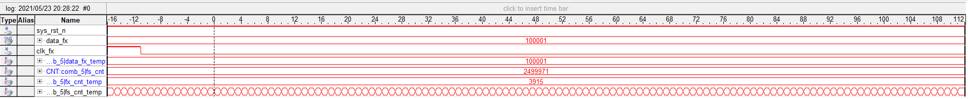
-待测时钟 100KHz

Signaltap测量值:100001Hz
-待测时钟 100Hz

Signaltap测量值:100Hz

-待测时钟输入:123456Hz
Signaltap测量值:123457Hz

结论
当输入待测方波信号赋值(实验测量使用的是5.0Vpp),测量结果准确稳定,能够在全频段实现比较精确的测量。
补充
上述实验测试的信号源输入方式很不安全,当信号幅度5Vpp,偏移0mV,意味着信号是2.5V的输出,而FPGA通常输入范围是0~3.3V,极限是-0.7V~4.0V
信号源输出的下限超出了FPGA允许的下限,是比较危险的,推荐的设置是输出3.3Vpp,偏移1.65V。


 2368
2368


 被折叠的 条评论
为什么被折叠?
被折叠的 条评论
为什么被折叠?
 到【灌水乐园】发言


