


Organic Light-Emitting Diodes ( OLEDs ) are the key component of modern displays with high contrast ratio, high level of sharpness, and stunning color gamut. Currently, researchers are also focusing on developing new Light-Emitting Diodes (LEDs), in which perovskites are used as emitting materials. Perovskite LEDs (PeLEDs) are getting more efficient by the day, also thanks to the extensive research on perovskite solar cells. The development of these devices has been possible only through an accurate electrical and optical characterization of both OLEDs and PeLEDs.
Typically, Organic and Perovskite Light Emitting Diodes (LEDs) are characterized only in steady-state to determine and optimize their efficiency. Adding further electro-optical measurement techniques in the frequency and time domain helps to analyze charge carrier and exciton dynamics and provides deeper insights into the physics of the device. In this tutorial, we present first an overview of frequently used measurement techniques and analytical models for OLEDs and perovskite LEDs. A multi-layer OLED with a sky-blue thermally activated delayed fluorescent (TADF) dopant material is employed in this study as a reference device.
The second part of this tutorial focuses on how to systematically fit the measured OLED characteristics with microscopic device simulations , based on a charge drift-diffusion and exciton migration model. Finally, we analyze the correlation and sensitivity of the determined material parameters and use the obtained device model to understand the limitations of the specific OLED device.
The combination of electrical characterizations and full device simulation allows one to determine specific material parameters, such as the charge carrier mobility of all layers.
All these characterizations can be performed with PAIOS. The simulations are carried on withSETFOS.
3. Characterization Techniques for Light Emitting Diodes (LEDs)
3.1. Current-voltage (JV) and JV-Luminescence (JVL) Characteristics
3.2 Impedance Spectroscopy (IS)
3.3. Transient Electroluminescence (TE)
3.6. Double Injection Transient (DIT)
3.7. Displacement Current Measurement (DCM):
3.8. Modulated Electroluminescence Spectroscopy (MELS):
2. Simulation Methods
3. Examples
Introduction
The newest display technologies could not be realized without the developments in organic light-emitting diodes (OLEDs). Despite their commercial success, there are still issues regarding the efficiency and lifetime of these devices to bring the technology to the next level. Similar (or more drastic issues) need to be resolved to develop a LED technology based on perovskite light-emitting materials. It is especially the blue LED that is lagging behind the performance and reliability of the green and red pixels. This affects the overall display operation, pixel layout choice, and performance.1 Therefore, it is important to better understand the device physics, in general, and the origins of degradation in OLEDs. Novel insight into the operating mechanisms will allow for the design and selection of new materials and provide guidance to optimize the device structure.
Besides the traditional solution or film characterization techniques, such as cyclic voltammetry2–4and ultraviolet photoelectron spectroscopy (UPS),5 new materials need to be thoroughly characterized in full multilayer LEDs or specific layer stacks to assess their suitability in real applications. This is also important as material properties may depend on the device fabrication details as well as the specific layer sequence. 6–10Thus, reliable material characterization in organic and perovskite LEDs is a key requirement. Yet, when devices are used as characterization test-beds, the material parameters are still extracted from single measurements on specific samples. This approach is time-consuming,requires high material consumption and the determined parameters are of limited validity because they might depend on the explicit device structure or on the peculiar analytical model that was selected to fit the data.11–13
The preferred way to determine material parameters in organic and perovskite LEDs should be, therefore, to combine numerical simulations with experiments. Often, these comparisons were solely focusing on steady-state analysis.14–16 In such cases, it is necessary to be careful that the analyzed material parameters are unique.17–19 In order to increase the reliability of device simulation, it is inevitable to include complementary measurement techniques in time and/or frequency domain.19–21
In the next section, we are going to present several techniques that are commonly used to characterize organic and perovskite LEDs. If we want to combine different measurement techniques to globally analyse an LED, it is crucial that all measurements are consistent, and that, systematic uncertainties introduced by individual measurement setups for each technique can be excluded. In the present study, this consistency is ensured by using the all-in-one measurement platform Paios which sequentially measures all electrical characteristics of one or several devices without the need to change the contact or the measurement system.23 In this way, any potential degradation between the different measurements can be reduced to a minimum or even completely excluded.
3. Characterization Techniques
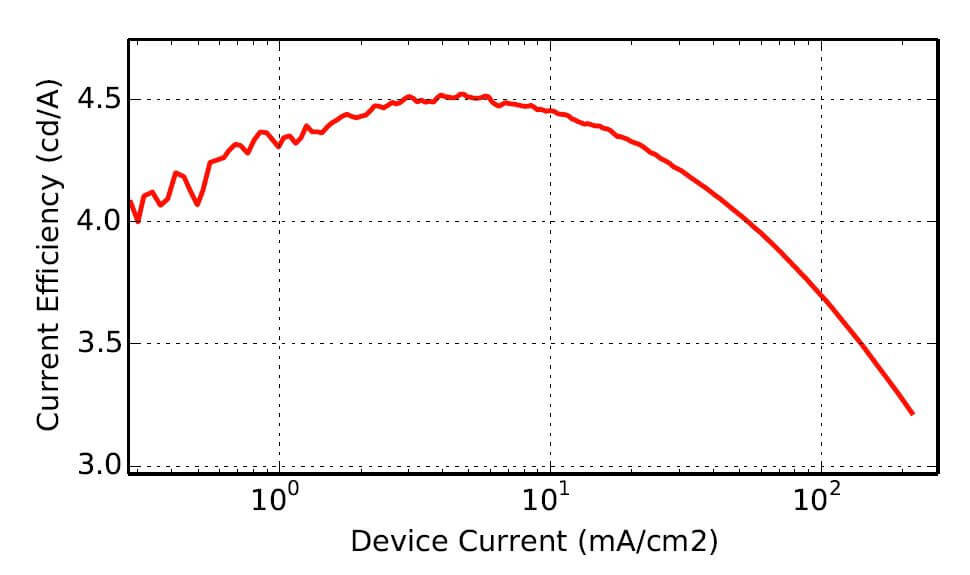
3.1 Current-Voltage-Luminance
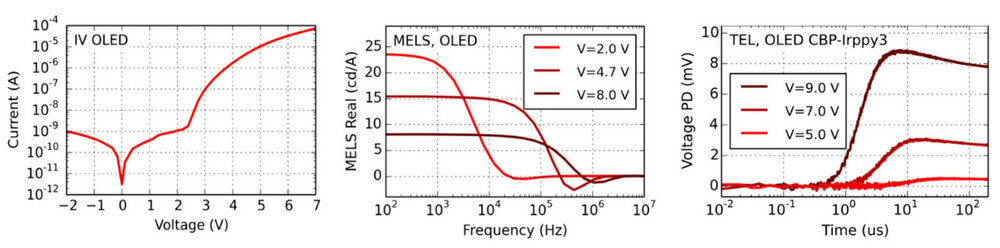
The current-voltage-luminance (IVL) measurement is the basic characterization method for OLEDs and perovskite LEDs.
The current-voltage curve is measured as in the normal IV. Additionally the steady-state emission of the OLED is recorded using a photodetector. Knowing the spectrum of the OLED and the sensitivity and geometry of the photodetector the electrical and optical efficiency of the OLED can be calculated.
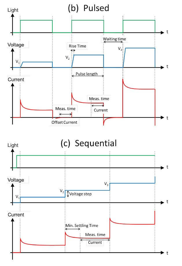
An accurate measurement is performed by using a pulsed voltage, as shown in the Figure. This means that in the best experiment, we are applying a certain voltage Vapp for around 80 ms and subsequently we switch back to 0 V before moving to the next voltage point. The current (luminance) at Vapp is averaged between 20 – 80 ms and the current (luminance) at 0 V is subtracted. Compared to the staircase (sequential) voltage scan, this method ensures reduced self-heating of the OLED and thus allows to go to higher current densities. Moreover, we can compensate for unintentional background light or for electrical noise in the light detection system.
This steady-state characterization is used to quantify the luminous efficiency, current efficacy or external quantum efficiency (EQE). Another interesting parameter which can directly be read from the measurement is the onset voltage (Vonset). In case of sufficient bipolar injection, the onset is usually related to the bandgap of the emitting layer (EML). 24 The obtained IV measurement can also be fitted by a single diode model to yield series Rs and parallel resistance Rp as well as reverse saturation current I0 and dark ideality factor n.
Parameters that can be extracted from this Analysis:
Emission Turn-On Voltage; Working Point; Single Diode Model.
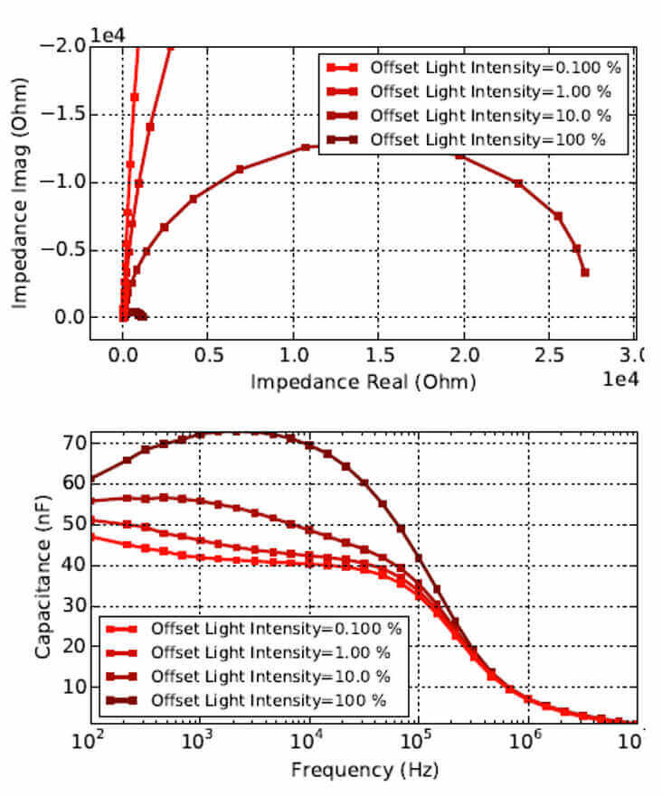
3.2. Impedance Spectroscopy
Impedance spectroscopy (IS) is often employed to study device properties of organic single-carrier devices, 19,25 solar cells 17,26–28 and OLEDs. 21,29,30. Recently, it was used also to characterize perovskite solar cells and LEDs. A voltage signal consisting of a steady-state bias V DC and an oscillating V AC part is applied to the device. The oscillating current I AC is measured and the resulting complex admittance Y (impedance Z) is calculated according to :
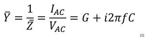
The representation of the IS data can vary. Typically, the conductance G and the capacitance C are evaluated from the real and imaginary part of the admittance, respectively. Either the steady-state voltage VDC is varied at a fixed frequency for or the frequency is varied at a constant V DC . Here we evaluate capacitance- (C- f ) and conductance-frequency (G- f) plots at different V DC . The amplitude of the oscillating voltage was always 70 mV. The benefit of considering the capacitance is that for interpretation of the data it can be related to the geometrical capacitance of the device and to parallel-plate capacitances of individual layers or set of layers. Another popular representation is the use of real and imaginary parts of the impedance Z. Moreover, the capacitive response can for instance be used to determine the relative permittivity of the organic materials, assuming the OLED to be well represented by a parallel plate capacitor. In specific cases there are analytical formulas that can be used to determine the charge carrier mobility. 19,31 Qualitatively, impedance data can also be used to investigate charge carrier injection, accumulation and trap states.17,19,21 ,25,26,29–33 Often,the impedance measurements are fitted by equivalent circuits. 28,29,34,35 In order to gain some knowledge on the operation principle of the investigated device, the individual elements of the electrical circuit have to be assigned to different layers and physical processes. Depending on on the complexity of the chosen equivalent circuit this assignment can be ambiguous. Reliable material parameter extraction is therefore challenging.Reliable material parameter extraction is therefore challenging.Reliable material parameter extraction is therefore challenging.
If you want to understand how to perform these measurements with PAIOS, just let us known
3.3 Transient Electroluminescence
Transient Electroluminescence can provide several information when used on an OLED or PeLED. It can provide insights about the charge carrier mobility and the luminescence lifetime.
For a transient electroluminescence (TEL) measurement, a rectangular voltage pulse V is applied to the OLED with varied amplitude. The length of the pulse is chosen such that steady-state conditions are reached at the end of the pulse. Both, the rise of the luminance signal as well as the decay can provide valuable insight into charge carrier and exciton dynamics in the OLED.
The measured characteristic onset time in the TEL signal can be related to the transit time t tr , ie the time it takes for the charge carriers to be injected and transported before meeting and recombining radiatively. Thus, the onset time directly reflects the two charge carriers mobilities of electrons and holes. An analytical relation between the transit time ttr and the charge carrier mobility µ is given by 36
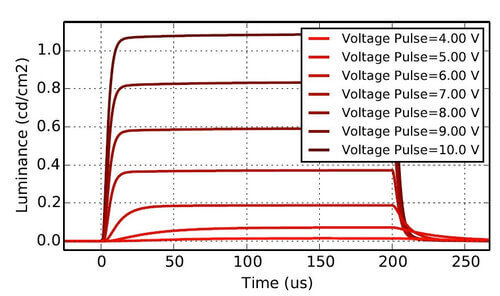
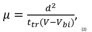
where d is the thickness of the device and Vbi the built-in potential. Usually the transit time is approximated by the delay time td between the voltage turn-on and the light onset which might lead to an overestimation of the mobility. 36 This simple formula was developed for single-layer devices which are not injection limited and neglects the spatial variation of the electric field due to the accumulated charge. 36–38 In multi-layer bipolar devices, the relevant thickness parameter d corresponds to the distance which the slower charge carrier needs to travel in order to meet and recombine with the counter-charge. Even though in state-of-the-art OLEDs the onset analysis only yields an apparent mobility, the technique can nevertheless be very useful to qualitatively understand basic charge transport phenomena.39 The analysis of the TEL rise dynamics is not discussed here in detail for sake of brevity, even though fast and subsequent slow rise can be assigned to the two carriers in the emission layer36 and sometimes a TEL onset overshoot can be observed due to rapid depletion of internally accumulated charges. 40
The TEL decay, however, is generally related to exciton dynamics and similarly interpreted to transient photoluminescence (TRPL). A single exponential decay fit yields an exciton lifetime that can be related to the radiative and non-radiative recombination rates. In contrast to TRPL also charge carriers are present in a TEL experiment. Therefore the decay can be affected by exciton-polaron interactions41 and delayed recombination of charge carriers. 20 Such TEL data have been analyzed in depth do understand different losses in OLED devices 20,42,43 as well as changes during device degradation. 44
Parameter that can be extracted from a TE analyis:
Luminescence Lifetime; Field Dependent Charge Carrier Mobility.
3.4 Injection CELIV
Charge extraction by linearly increasing voltage (CELIV) has first been presented as an analysis technique for inorganic solar cell devices. 45,46 In this experiment, mobile charge carriers that are present in the device are extracted by a reverse voltage ramp (triangular pulse) . The associated current is composed of a constant displacement current and an overshoot which is related to the extracted charge carriers. Depending on the way that charge carriers are generated inside the device, one can distinguish between dark- (doping), photo- (light pulse) and injection-CELIV (offset voltage). While the second is commonly used for organic solar cells 11,13,26,47,48 the last is mostly employed in metal-insulator-semiconductor (MIS) devices as well as in OLEDs . 30,49,50 It is also suitable for the analyis of perovskite LEDs.
 最低0.47元/天 解锁文章


 2776
2776


 被折叠的 条评论
为什么被折叠?
被折叠的 条评论
为什么被折叠?
 到【灌水乐园】发言


