


Microelectromechanical systems (MEMS) are systems that integrate miniature mechanical and electronic components with sensing, control, and actuation functions.MEMS products are widely used in automotive, medical, communications, aerospace, and other fields. Due to the complex structure and tiny size of MEMS products, their packaging and interconnection technologies have an important impact on their performance and reliability, as shown in Figure 1.
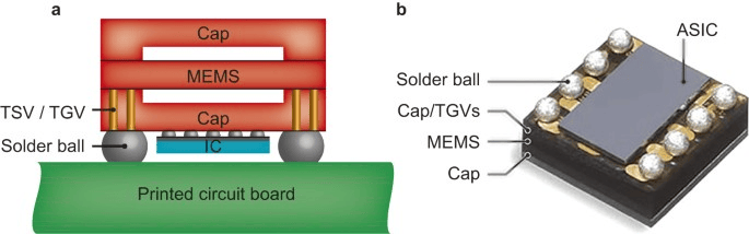
Figure 1. Integrated MEMS
Traditional reflow soldering is widely used as a flux-based solder balling process for creating solder bumps and interconnects for microelectronic packages. An adhesive flux is applied to the metal pads prior to the reflow process to hold the solder balls in place after initial placement. In addition, the flux removes the oxide layer from the surface of the metal pads and promotes solder wetting during the reflow process.
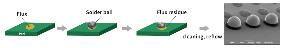
Figure 2. Conventional Ball Placement Soldering Process
A chemical reaction occurs between the solder balls and the metal bonding pads to form a continuous intermetallic compound (IMC) layer at the bonding interface. Due to the low activation energy of the IMC layer, the IMC layer continues to grow through a solid-state diffusion mechanism even if the tin balls are completely solidified at room temperature. However, IMC is inherently brittle and an excessively thick IMC layer can deteriorate the mechanical integrity of the solder joint and affect the long-term reliability of the assembled electronic package. Although flux-based solder ball soldering processes are widely used due to their reliability and simplicity of execution, flux and ball placement is typically limited to interconnect spacing/ball placement tooling greater than 200 μm, directly matched to the metal pads of the package, due to manufacturing accuracy limitations in the layout of the fine openings in the flux.
In addition, several mechanical handling steps of conventional reflow soldering, such as applying flux, placing solder balls, and cleaning residual flux, can cause damage to sensitive devices in optoelectronic and microelectromechanical systems (MEMS) packages. The entire packaging process is exposed to high temperatures in the reflow oven, which is detrimental to thermally sensitive devices. In addition, solder joints may fail due to a mismatch in the coefficient of thermal expansion.
As the microelectronics industry continues to pursue miniaturization and better performance, the input/output count density of electronic packages within a given area is increasing. Conventional flux-based ball placement processes are quickly reaching a bottleneck in meeting tighter pitch tolerances and assembly challenges in optoelectronics and MEMS packages. In response to the new packaging demands, flux-free laser solder ball jetting technology has been developed.
Laser solder ball jetting is a highly flexible, flux-free solder ball attachment process with low heat and no mechanical stress on the packaged device. Compared to conventional reflow soldering, laser ball jetting has a higher energy input and localized heating capability, making it ideal for high-temperature solder ball alloys. The energy of the laser pulse is absorbed by the solder balls, causing them to melt and wet onto the metal pads while avoiding heat-related problems.
Advantages of this technology include:
1. No flux, avoiding contamination and corrosion of packages and devices from flux residues.
2. The diameter and spacing of the solder balls can be flexibly adjusted for different package designs and requirements.
3. The energy and time of the laser beam can be precisely controlled, realizing local heating and rapid cooling, reducing thermal stress and thermal deformation.
4. The laser solder ball spraying process does not require contact, avoiding mechanical damage and contamination of the package and device.
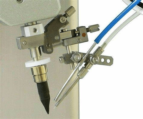
Figure 3. Laser welding technology
In summary, laser solder ball jetting technology is an advanced flux-free solder ball attachment process with high efficiency, reliability, flexibility and environmental protection, which is suitable for packaging and interconnection of microelectromechanical products, providing a guarantee for the performance and quality of microelectromechanical products.


 402
402

 被折叠的 条评论
为什么被折叠?
被折叠的 条评论
为什么被折叠?
 到【灌水乐园】发言


