


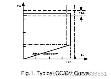
PL3328BD is a series of high efficiency Primary Side Regulator and highly integrated PWM Power Switch for AC/DC power supply applications. It simplifies conventional CC/CV charger/adaptor designs by eliminating the opto-coupler and secondary control circuitry. Very tight output voltage and current regulation is realized as shown in the Fig.1 below. During operation, multi-mode operations are utilized to achieve low standby power, high efficiency and audio & noise free. The integrated Power MOSFET could reduce external components and system cost. PL3328BD also offers rich protection features including Cycle-by-Cycle peak current limiting, UVLO, OVP. The switch continues attempting start-up until the fault condition is removed. Every restart is a soft start.
Overview
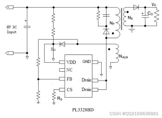
PL3328BD is a primary side CC/CV regulator designed for high performance offline Switch Mode Power Supplies with minimal external components. The device is integrated high voltage power switching regulators which combines an avalanche rugged Sense FET with a primary side control block. PL3328BD is designed for AC/DC applications. And it provides accurate current/voltage without requiring the opto-coupler and the secondary control circuitry. It also eliminates the need of loop compensation circuitry while maintaining stability. thus, very tight output voltage and current regulation is achieved.
PL3328BD’s multi-mode operations are utilized to achieve low standby power, high efficiency
and audio & noise free. in CC mode as well at large load condition, it operations in PFM mode, while at light load or medium load,PL3328BD works in PWM with frequency reduction. This green-mode function assists the power supply meeting the power conservation requirements. A complete set of integrated protection functions allows PL3328BD to protect against all fault conditions including Cycle-by-Cycle peak current limiting, VDD UVLO, OVP . The switch continues attempting start-up until the fault condition is removed.
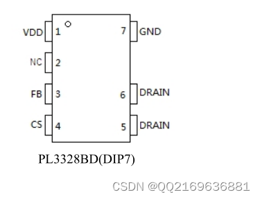
PL3328BD is offered in DIP-7 package.
Features
Built-in Integrated Power MOSFET
+/-5% Constant Voltage Regulation
Accurate Constant Current Regulation at Universal AC input
Eliminates Opto-coupler and all Secondary CV/CC Control Circuitry
Built-in Line Compensation for Tighter CC Regulation
Built-in Compensation for Transformer Inductance Tolerances
Adjustable Output Cable Compensation
Adaptive Multi-mode PWM/PFM Control for Improving Efficiency
Low Start-up Current
LEB
OCP
OVP
Good dynamic response
UVLO
The pin map is shown as below .
Application Notes
PL3328BD provides a cost effective solution for low power adaptor/charger applications. The innovative CV and CC control can remove the need for secondary feedback circuitry while achieving excellent CV/CC for much more strict requirements.
Startup & Operating Current
PL3328BD has very slight startup current , thus the larger value startup resistor and smaller VDD capacitor can be used to minimize the power loss in application. The operating current of PL3328BD is as low as 1mA. Together with ‘Muti-mode’ control features we could get high efficiency especially in light load.
Under Voltage Lockout (UVLO)
An UVLO detector is implemented in it to detect the voltage on the VDD pin. It would assure the supply voltage enough to turn on the PWM controller and further to drive the power mos. a hysteresis is built in to prevent the shutdown from the voltage dip during startup. The turn-on
and turn-off threshold level are set at 16 V and 8 V, typically.


 442
442


 被折叠的 条评论
为什么被折叠?
被折叠的 条评论
为什么被折叠?
 到【灌水乐园】发言


