


How to generate Gerber and Drill files in KiCad 4
Generate Drill and Gerber Files
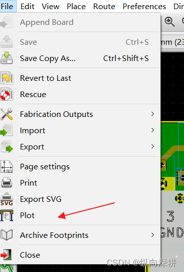
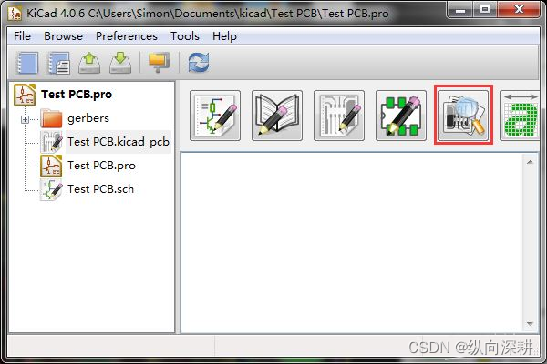
Select File -> Plot from the menu to open the gerber generation tool.
In general, there are 8x layers you need to have a PCB fabricated:
Top Copper (F.Cu)+ Soldermask (F.Mask) + Silkscreen (F.SilkS)
Bottom Copper (B.Cu) + Soldermask (B.Mask) + Silkscreen (B.SilkS)
Board outline (Edge.Cuts)
Drill file
In the Plot window with the Plot format set for Gerber, be sure these Layers are checked:
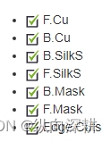
If you don’t know which layers, please check all layers, JLCPCB will help you to use the right layers. Click ‘Plot’ to generate the gerber files for the layers.
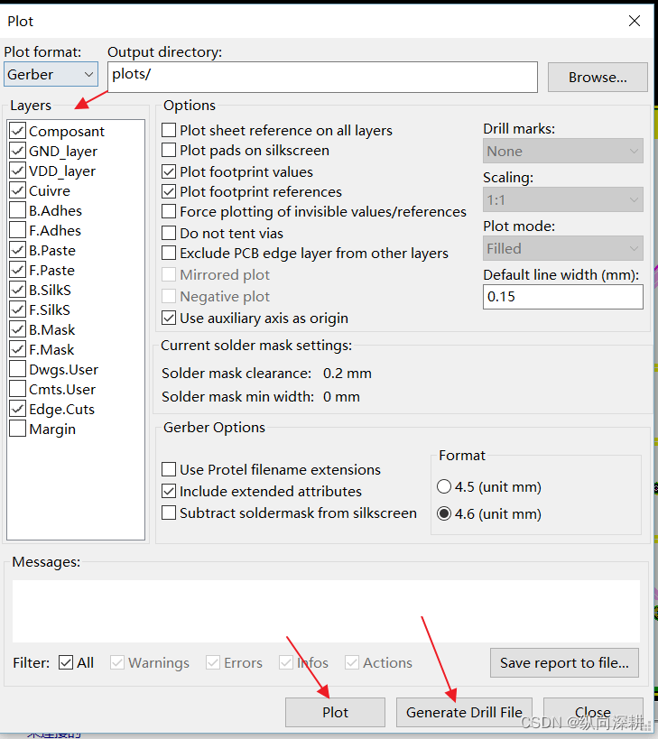
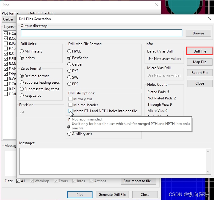
Don’t forget to Generate the Drill Files. Click on ‘Generate Drill File’ button. You can use the defaults here as well. Check the “Merge PTH and NPTH holes into one file” box. For now just click ‘Drill File’ or press ‘enter’ to generate the drill file. Use the same output folder as for the gerbers, which should be the default.
Check the Gerber files in GerbView
Next, click ‘Close’to exit the Drill and Plot windows. All of the files should have appeared in your gerbers folder. KiCAD comes with a gerber viewer called GerbView, you can open the “GerbView” and check what your board looks like before sending it to manufacturer.
For more details, please see this video tutorial of generating Gerber files for manufacturing in KiCad.
For Kicad 5.1.9, please check this tutorial.
If everything looks OK, select all of the files, zip them up, and upload the zip file to JLCPCB order page.


 1889
1889


 被折叠的 条评论
为什么被折叠?
被折叠的 条评论
为什么被折叠?
 到【灌水乐园】发言


