


写在前面
本系列文章主要讲解德州仪器(TI)TDA4VM芯片的相关知识,希望能帮助更多的同学认识和了解德州仪器(TI)TDA4VM芯片。
若有相关问题,欢迎评论沟通,共同进步。(*^▽^*)
错过其他章节的同学可以电梯直达目录↓↓↓
TDA4VM芯片
6. 时序和开关特性
6.2 电源时序
6.2.5 隔离MCU域和主域的下电时序
图7描述了隔离MCU域和主域的下电时序。
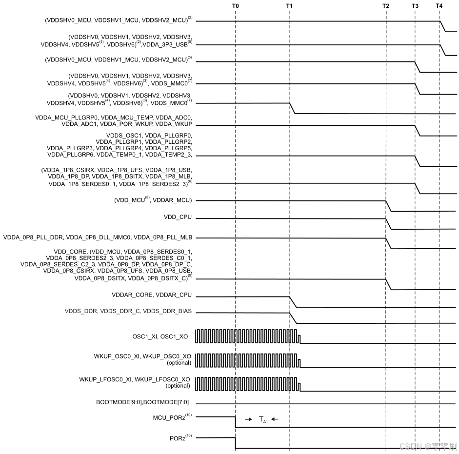
图 7 隔离MCU域和主域的下电时序
1. 时间戳标记
T0 – MCU_PORz & PORz assert low to put all processor resources in safe state. (0ms)
T1 – Main DDR, SRAM Core & SRAM CPU power supplies start ramp-down. (0.5ms)
T2 – Low voltage core supplies start supply ramp-down. (2.5ms)
T3 - 1.8V voltages start supply ramp-down. (3.0ms)
T4 – 3.3V voltages start supply ramp-down. (3.5ms)
2. Any MCU or Main dual voltage IO supplies (VDDSHVn_MCU or VDDSHVn) being supplied by 3.3V to support 3.3V digital interfaces.
3. Any MCU or Main dual voltage IO supplies (VDDSHVn_MCU or VDDSHVn) being supplied by 1.8V tosupport 1.8V digital interfaces. When eMMC memories are used, Main 1.8V supplies could have a ramp-down aligned to T1 due to PDN designs grouping supplies with VDD_MMC0.
4. VDDSHV5 supports MMC1 signaling for SD memory cards. A dual voltage (3.3V/1.8V) power rail is requiredfor compliant, high-speed SD card operations. If compliant highspeed SD card operation is needed, then an independent, dual voltage (3.3V/1.8V) power source and rail are required. The start of ramp-down from 3.3V/1.8V will be same as other 3.3V domains as shown. If SD card is not needed or standard data rates with fixed 3.3V operation is acceptable, then domain can be grouped with digital IO 3.3V power rail. If a SD card is capable of operating with fixed 1.8V, then domain can be grouped with digital IO 1.8V power rail.
5. VDDA_3P3_USB is 3.3V analog domain used for USB 2.0 differential interface signaling. A low noise,analog supply is recommended to provide best signal integrity for USB data eye mask compliance. The start of ramp-down from 3.3V will be same as other 3.3V domains as shown. If USB interface is not needed or data bit errors can be tolerated, then domain can be grouped with 3.3V digital IO power rail either directly or through a supply filter.
6. VDDA_1P8_<phy> are 1.8V analog domains supporting multiple serial PHY interfaces. A low noise, analogsupply is recommended to provide best signal integrity, interface performance and spec compliance. If any of these interfaces are not needed, data bit errors or non-compliant operation can be tolerated, then domains can be grouped with digital IO 1.8V power rail either directly or through an in-line supply filter is allowed.
7. VDD_MMC0 is 1.8V digital supply supporting MMC0 signaling for eMMC interface and must ramp-down attime stamp T1 before VDD_CORE starts ramp-down. Any MCU or Main dual voltage IO operating at 1.8V can be grouped with VDD_MMC0 into a common power rail with power down time stamp T1. If MMC0 or eMMC0 interface is not needed, then domain can be grouped with digital IO 1.8V power rail and ramp-down at time stamp T3.
8. VDD_MCU is a digital voltage supply with a wide operating voltage range and power sequencing flexibility,enabling it to be grouped and ramped-down with either 0.8V VDD_CORE at time stamp T2 or 0.85V RAM array domains (VDDAR_xxx) at time stamp T1.
9. VDDA_1P8_<clk/pll/ana> are 1.8V analog domains supporting clock oscillator, PLL & analog circuitryneeding a low noise supply for optimal performance. It is not recommended to combine analog VDDA_1P8_<phy> domains or digital VDDSHVn_MCU and VDDSHVn IO domains since high frequency switching noise could negatively impact jitter performance of clock, PLL and DLL signals.
10. MCU_PORz and PORz must be asserted low for TΔ1 = 200us min to ensure SoC resources enter into safestate before any voltage begins to ramp down.
6.2.6 仅MCU进入和退出状态
进入MCU仅通过执行电源关闭时序来实现,除了4个MCU电源组(VDDSHVx_MCU在3.3V,VDDSHVx_MCU在1.8V,VDDA_MCU_PLLGRP0/VDDA_MCU_TEMP模拟电源在1.8V,VDD_MCU/VDDAR_MCU在0.85V)保持供电外。从MCU仅状态退出是通过执行电源开启时序实现的,在整个时序中保持4个MCU电源组供电。如图8所示用于具有eMMC支持的隔离MCU域和主域PDN类型。
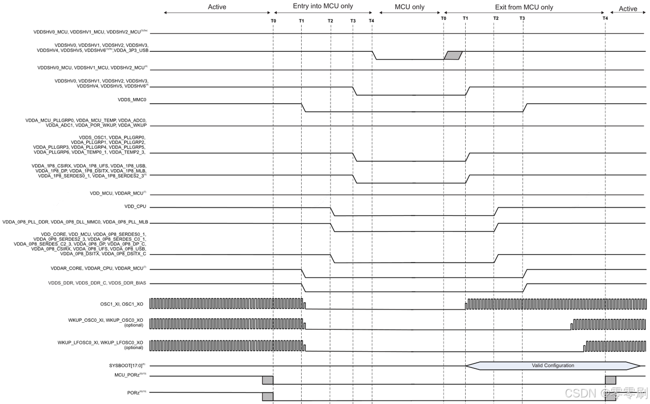
图 8 仅MCU进入和退出的时序
6.2.7 DDR保留状态的进入和退出
进入DDR保留(Suspend-to-RAM或S2R)状态是通过执行一个电源关闭时序来完成的,除了1个设备DDR供电组(VDDS_DDR_BIAS,VDDS_DDR和VDDS_DDR_C,电压为1.1V),以及1个额外的独立SDRAM供电(VDD_LPDDR4_1V8,电压为1.8V;在下面的图中未显示)保持供电。退出DDR保留状态是通过执行一个电源开启时序来完成的,这两个DDR供电组在整个时序中保持供电。如图9所示用于具有eMMC支持的隔离MCU域和主域PDN类型。

图 9 DDR保留状态进入和退出的时序
本文章是博主花费大量的时间精力进行梳理和总结而成,希望能帮助更多的小伙伴~ 🙏🙏🙏
后续内容将持续更新,敬请期待(*^▽^*)
欢迎大家评论,点赞,收藏→→→


 被折叠的 条评论
为什么被折叠?
被折叠的 条评论
为什么被折叠?
 到【灌水乐园】发言


