


REF
eFuse
1 Need for Protection and Ways to Achieve
Modern electronic systems are designed with high level of integration to offer superior performance with multitude of functionality. These systems use multi-voltage power distribution to support various types of loads for their proper operation. One of the major expectations is the minimal system downtime during any transient abnormal events such as overload or short-circuit conditions. For example, while hot-plugging a hard disk drive into a storage system, huge inrush current can result in voltage sag on the connected bus and eventually affect other operating loads on the same bus. To overcome this scenario, today’s system designers use protection devices to manage inrush, overload, short circuit, and overvoltage events and to guard the sensitive loads for reliable system operation. The key requirement is to bring down the fault currents within the limits and bring the system back to active state once the fault is cleared, without any manual intervention.
Fuses, positive temperature coefficient (PTC) resistors, and active circuit protection are a few of the protection devices with varied capabilities and drawbacks. Fuses are traditionally considered as protection devices used to isolate overload or short-circuit faults from the main system. Although these devices provide protection, the fault current needs to be exceedingly higher than the rating of the fuse with response time ranging from milliseconds to seconds. This makes it extremely difficult to predict the precise overcurrent level at which the fuse will open. A conservative selection on fuse current rating may lead to fuse blowup during inrush current events. In addition, once the fuse blows during an overload event, it has to be physically replaced, which increases system down time and maintenance costs. On the other hand, PTC resistors provide resettable overcurrent protection and, unlike a fuse, these can avoid the physical intervention. However, because they are actuated by the heating effect of an overcurrent load, their reaction time is limited to several milliseconds. Also the ON-resistance of PTC fuse increases after every reset, which raises concerns on achieving repeatable performance over time.
The best way to prevent system downtime is to detect, respond and correct potentially damaging conditions as quickly as possible. As the response of fuse and PTC resistors depends on heating effect (temperature, a lagging parameter) for their operation, many system designers prefer to use a leading indicator, current, to provide effective circuit protection. Both fuse and PTC resistors do not cover many of the protection requirements such as inrush control, overvoltage; reverse current, reverse polarity protections needed in modern electronic systems. The next section describes the active circuit-protection solutions using discrete components and the challenges involved.
2 Discrete Circuit-Protection Solutions
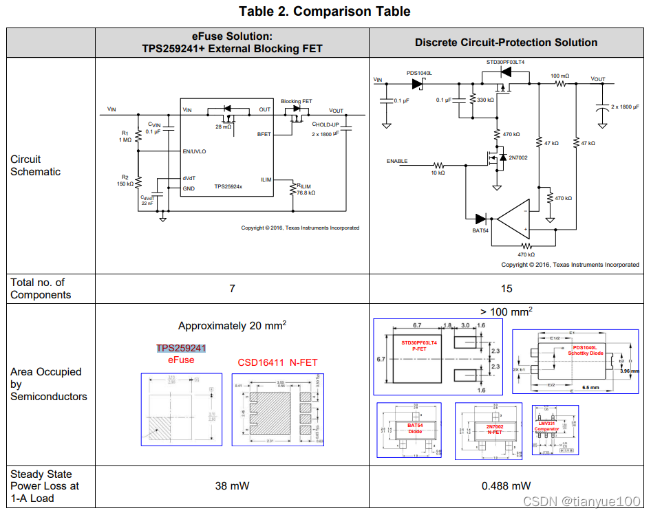
Many of the discrete circuit-protection solutions use a combination of fuses, diodes, MOSFETs, and TVS diodes to meet a specific protection requirement. A typical discrete circuit using a combination of fuse and MOSFET is shown in Figure 1. The protection circuit incorporates inrush current control using P-MOSFET, a series diode to block the reverse current as well as reverse polarity, a fuse for overload or short-circuit protection, and comparator logic to disconnect the power path during undervoltage or overvoltage events. The inrush current limiter avoids voltage sag on the connected bus during hot plug events and helps in optimal fuse-sizing for a precise overcurrent level. However, challenges with current-limit inaccuracies with temperature and slower response still exist. An active current-protection circuit shown in Figure 2 can respond faster to overcurrent faults and provides better current-limit accuracies. However, many of the discrete circuit-protection realizations have the following shortcomings which limit their wider usage:
• Discrete circuits use P-MOSFET as pass FET, which is more expensive than N-MOSFET to achieve the same ON resistance (RDS(ON)).
• Discrete solutions are bulky and inefficient. For example, a 2-A load current results in around 1.4-W power dissipation across the diode and corresponding rise in board temperature.
• Discrete circuits do not incorporate thermal protection for the pass FET. So the thermal design is often more oversized than safe operating area (SOA) limits for device protection under extreme cases.
• A discrete circuit needs more components and occupies more board space. More components also raise concerns on protection-circuit robustness and reliability.
• Though the output voltage slew rate is adjustable with RC components, these components must be sized in consideration with the gate characteristic of the pass FET.


3 What is an eFuse?
An integrated circuit protection solution called “eFuse” can overcome the limitations with discrete circuit protection realizations. An eFuse is an “active circuit protection device with an integrated FET used to limit currents, voltages to safe levels during fault conditions”. It embeds various functions to protect system against inrush current, overcurrent, overvoltage, reverse current, reverse polarity and short circuit faults. The eFuse is more accurate, faster and can ‘repair’ itself without user intervention. Most of the TI eFuses are recognized as Solid State Overcurrent Protectors under the UL2367 standard. Also these are certified under safety standard UL 60950 and are safe to use.
Figure 3 shows a block diagram of an eFuse. An understanding of the functionality of various features in an eFuse helps in choosing the right eFuse for a particular application. This section discusses the functionality of each feature the eFuse offers. As shown in Figure 3, an eFuse requires very few external components (resistor RILIM for current limit setting and a capacitor CdVdT for setting the output voltage ramp rate) resulting in significant board space saving and robust protection when compared to discrete solutions.

3.1 Inrush Current Control
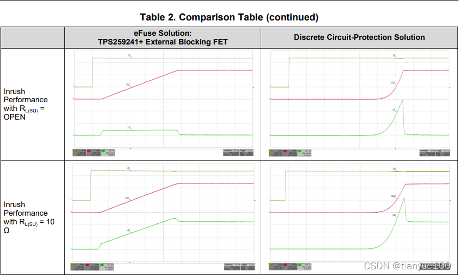
Inrush currents are a major concern in DC power systems. For example, while hot-plugging a hard disk drive into a storage system, huge inrush current can result due to quickly charging its filter or load capacitor. This huge inrush current with fast slew rate causes voltage sag on the backplane which could affect operation of other connected loads. This problem can be solved by controlling the output voltage ramp rate, thereby limiting the inrush current and disturbance on the backplane. Discrete circuits (Figure 1, Figure 2) use RC components around pass FET for inrush current control, which must be sized in consideration with the gate characteristic of the pass FET and the load. Sometimes, it needs many design iterations to keep inrush current within the desired limit. If the input power is cycled rapidly, the load capacitor gets discharged quickly while the external gate capacitor remains charged and maintains pass FET in the ON condition. This inhibits the current-limiting feature allowing a large current surge when power is restored.
In an eFuse, the output voltage ramp rate is inversely proportional to the CdVdT capacitor value and can be configured easily at the desired rate. The built-in overtemperature protection in an eFuse prevents device failure that could happen due to severe dynamic power stress during startup. Refer to Section 4 for the inrush performance comparison between eFuse and a discrete solution.
3.2 Overcurrent Protection
When an overcurrent event happens, protection for the downstream circuitry from excessive currents is essential to avoid any potential circuit damage or fire. The active current protection circuit shown in Figure 2 uses an external current sense resistor and a fast comparator for overcurrent protection. This circuit realization often needs tradeoff between accuracy, cost, and power loss. TI eFuses provide active current protection either by limiting the fault current (called current-limiting operation) or by breaking the fault circuit after an overload timeout (called circuit-breaker operation). The latest devices, such as the TPS25942 and TPS25944, offer ±8% current-limit accuracy over the load range of 0.6 A to 5.3 A.
An eFuse with the current-limiting feature limits the output current to a threshold set by an external resistor RILIM. Figure 4 shows the current-limit response of the TPS25942A eFuse, with the current limit (ILIM) set to 5 A. For an overload condition, the eFuse limits the input current to 5 A until either the overload is removed or the eFuse junction temperature TJ reaches thermal shutdown temperature (typically TTSD = 150°C). Once the eFuse enters thermal shutdown, it either remains in the OFF position (a latch-off version) or attempts to restart after TJ falls below TTSD by 12°C and with auto retry delay (128 ms for TPS25942A, an auto-retry device). It is observed in Figure 4, the TPS25942A makes circuit closure after every thermal shutdown and finally restores to normal condition when the overload fault is cleared. The current-limiting feature is beneficial in applications such as solid-state drives (SSDs), especially if the overcurrent event is temporary and to avoid system downtime.
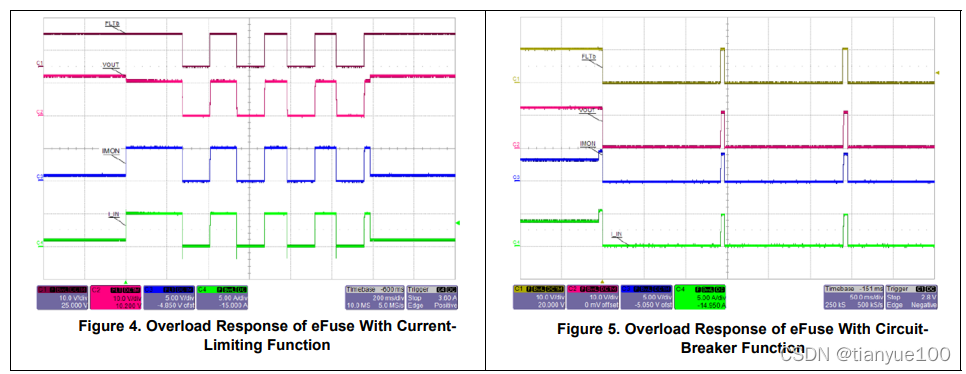
For sensitive loads, such as a hard drive in data servers, an immediate power path opening is a safe option in response to an overcurrent fault. An eFuse TPS25944A provides circuit-breaker operation with overload timeout. When the load current exceeds the set current limit of 5 A, the TPS25944A starts the fault timer and breaks the circuit path if the load current does not fall below ILIM before the fault timer expires (4 ms). Figure 5 shows circuit-breaker response of the TPS25944A eFuse, and since the TPS25944A is an auto retry device, it attempts to restart after a circuit-breaker retry delay of 128 ms. The circuit-breaker feature essentially avoids system downtime by allowing pulsed overloads at the output for a fault period interval of 4 ms..
3.3 Short-Circuit Protection
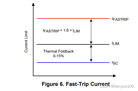
One of the advantages of an eFuse over discrete solutions is the ability to respond faster for hot-short faults at the output. During a transient short-circuit event, the current through the eFuse increases very rapidly. The current-limit amplifier of an eFuse cannot respond very quickly due to its limited bandwidth. TI eFuses incorporate a fast-trip current comparator, which shuts down the pass FET very quickly when the load current IOUT > fast-trip current threshold IFASTRIP. This terminates the rapid short-circuit peak current in less than 200 ns as shown in Figure 8. The fast trip threshold is set to 60% higher than the programmed overload current limit (IFASTRIP = 1.6 × ILIM). After the transient short-circuit peak current has been terminated by the fast-trip comparator, the current-limit amplifier smoothly regulates the output current to ILIM as shown in Figure 7. If during current-limit operation, power dissipation of the pass FET [(VIN – VOUT) × IOUT] exceeds 10 W, there is approximately a 0 to 15% thermal fold back in the current-limit value so that ILIM drops to ISC. Eventually, the device shuts down due to over temperature.

3.4 Reverse Current Protection
Reverse currents can flow through the system when the voltage at the output is higher than at the input. In applications such as power muxing for redundant power systems or SSD with a large hold-up output capacitor, there is a risk of large reverse currents when the input power is disconnected. The reverse current can damage internal circuitry or system power supplies, if it is not limited. For certain applications such as PLC controller modules, this feature is mandatory to pass ‘voltage interruption tests’.
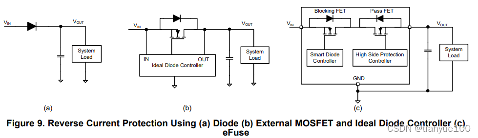
A series diode can block reverse currents but results in significant power loss in the system which could lower the system efficiency and battery life. An external MOSFET with an ideal diode controller IC (shown in Figure 9(b)) is a more efficient option and also offers flexibility in current support; however, it occupies more board space. TI's TPS2594 family of eFuses integrates blocking FET and a fast reverse comparator to provide true reverse current blocking. When an input power fail condition is detected, the internal FET is turned OFF in 1 µs (typical). True reverse current blocking facilitates simplified efficient power muxing in redundant power systems. For additional information regarding power multiplexing using eFuses, see reference (1).
3.5 Overvoltage Protection
Transient induced voltages or inductive switching can cause overvoltage in the system which lasts from a few hundred microseconds to milliseconds. An eFuse with output voltage-cutoff guards the sensitive circuits from overvoltage by turning OFF the internal FET. The trip point for overvoltage cutoff can be programmable through an external resistor at the OVP pin of eFuse. As shown in Figure 10, the TPS25942x remains active for a nominal 12-V input voltage. When the input voltage exceeds the overvoltage trip point (16.5 V here), the eFuse turns OFF the internal FET causing the output voltage VOUT to fall to zero. The eFuse remains in the OFF condition as long as the input voltage exceeds the set overvoltage trip point. Once the input voltage returns to nominal operating voltage, the device turns back ON and VOUT once again returns to 12 V. The latest eFuse device, TPS2660, protects the load up to 60-V DC Safe Extra Low Voltage (SELV) faults and is suitable for industrial applications.
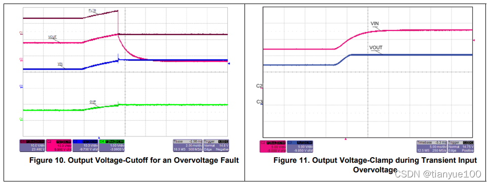
Some of the TI eFuses have an output voltage-clamp (OVC) feature, which keeps eFuse in operation by clamping the output voltage to the nominal voltage. As shown in Figure 11, the TPS25926x eFuse integrates a 15-V output voltage-clamp. When the input voltage exceeds the internal OVC trip point, the internal clamping circuitry activates and limits the output voltage to 15.6 V (typically 15 V). If the transient on the input is only temporary, the eFuse hides the overvoltage fault from downstream circuitry. If the fault lasts long enough to activate the eFuse’s thermal shutdown (typically TJ = 150°C), then the fault will still cause the eFuse to turn OFF (similar to output voltage-cutoff).
3.6 Over Temperature Protection
Discrete protection realizations need careful selection of pass FET and thermal design to keep the device in SOA limits under any extreme fault conditions. However, TI eFuses come with inbuilt over temperature protection and gets shutdown if the eFuse junction temperature, TJ , exceeds 150°C (typ). Once eFuse enters thermal shutdown, it either remains in the OFF position (a latch-off version) or attempts to restart (an auto retry version) after TJ falls below TTSD by 12°C and with auto retry delay.
3.7 Fault Response and Recovery
TI eFuses are available in two versions; latch off and auto retry. A latch-off version remains in the OFF position and needs power recycle to turn ON again. A system with the latch-off version provides more safety by immediately isolating the faulty component but also reduces the system uptime. Figure 12 shows the short-circuit response of the latched device TPS25942L, where the device provides a limited current of 5 A before getting into thermal shutdown. A reset at the enable pin is required to bring the device back into operation. On the other hand, a device with auto retry continues to power cycle itself until the fault is cleared. As shown in Figure 13, the device TPS25942A attempts to power cycle after retry delay (128 ms) and resumes normal operation when short circuit is cleared. Since, over-temperature protection is inbuilt, no special thermal considerations are required for surviving a prolonged output short.

3.8 Input Reverse Polarity Protection
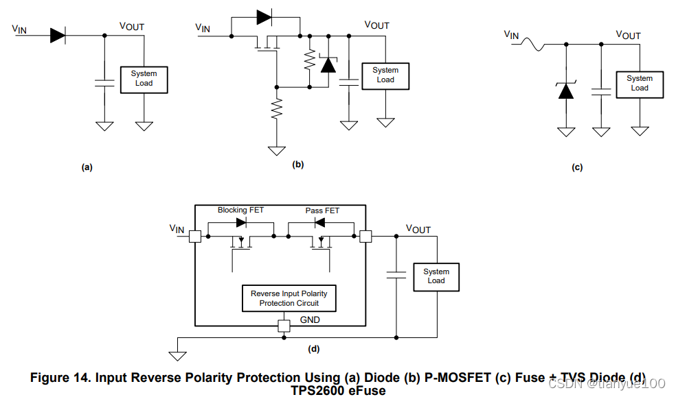
In applications such as PLC systems, the input side needs reverse polarity protection against any field supply mis-wiring. A blocking diode is the simplest means of protecting against reverse polarity connections. Since no control signal is required, circuit complexity and component count are low. On the other hand, the diode dissipates energy all the time due to its forward voltage (VF ) drop, which can cause significant power loss in high-current applications and needs thermal management. Another approach is to use a P-MOSFET, which can be implemented with simpler drive circuitry comprising a Zener diode and a resistor, as shown in Figure 14(b). A P-MOSFET based solution is expensive and has the risk of failure when the input power is removed causing the output capacitor discharge through the fully enhanced PMOSFET. Another simple solution, shown in Figure 14(c), uses a combination of fuse and TVS diode, where the fuse blows and protects the load against reverse polarity. But after the fault, the fuse needs to be replaced. As shown in Figure 14(d), the TI eFuse TPS2660 integrates a reverse input polarity protection circuit and does not need any external components. The TPS2660 ensures that the device is not functional during reverse polarity conditions and internal FET blocks the reverse current path.
3.9 Surge Protection
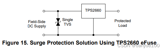
The TPS2660 eFuse-based surge protection solution (reference (2)) is shown in Figure 15. It requires only a single TVS diode to protect the load from surges. The device does not need any passive wave shaping circuits to reduce the slew rate of the surge. It can handle slew rates as fast as 20 V/µs. Built-in back-toback FETs and reverse polarity protection circuits effectively block negative voltage that can be generated due to a negative surge. The ±70-V transient absolute maximum ratings of the TPS2660 device enable the use of a single TVS diode for clamping the surge. Overvoltage and undervoltage protection makes sure that the downstream converters are isolated from input when the surge is at peak or valley level. A proprietary high-speed protection algorithm immediately disconnects the output from the input and prevents the surge passing from the input to the output.
3.10 Controlled Power Down
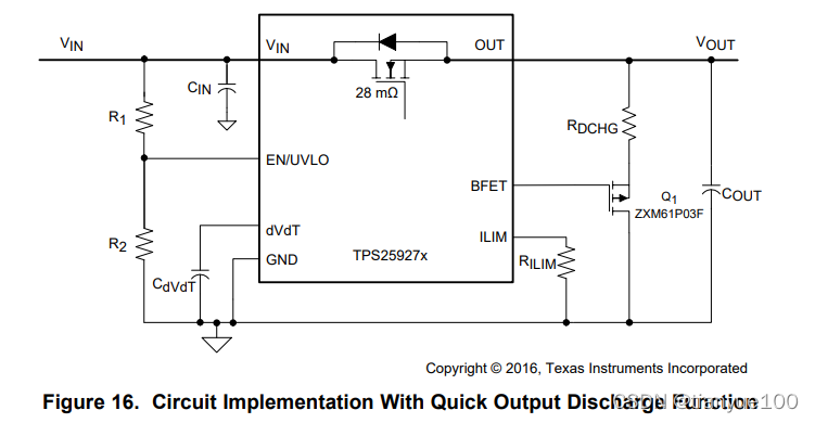
When the device is disabled, the output voltage is left floating and power down profile is entirely dictated by the load. In some applications, this can lead to undesired activity as the load is not powered down to a defined state. Controlled output discharge can ensure the load is turned OFF completely and not in an undefined operational state. The BFET pin in the TPS25927x family of eFuses facilitates the quick output discharge (QOD) function as illustrated in Figure 16. When the device is disabled, the BFET pin pulls low which enables the external P-MOSFET, Q1 , for the discharge feature to function. The output voltage discharge rate is dictated by the output capacitor, COUT, the discharge resistance, RDCHG, and the load.
3.11 UL Certifications
Most of the TI eFuses are UL 2367 (solid-state overcurrent protectors) recognized which would help in designing sections of the system as “limited energy” or “low power” circuits to expedite the UL certification process. Additionally, these devices are also UL 60950 (safe during single-point failure) recognized, which restricts the voltage, current within the circuit limits under any single fault. For additional information regarding benefits of UL recognition, the reader is directed to reference (3).
3.12 Additional Features
3.12.1 Health Monitoring and Reporting
The TPS2594xx family of eFuses provide advanced features such as precise load current monitor, voltage monitoring, and fault flag. The current source at the IMON terminal of the TPS2594xx eFuse is configured to be proportional to the current flowing through the device. A resistor from this pin to GND converts current to proportional voltage, which can be used as a means of monitoring the health of the system. The power good comparator has an internal reference of V(PGTHR) = 0.99 V at the negative terminal and the positive terminal PGTH can be utilized for monitoring of either input or output of the device or any other voltage rail in the system. The comparator output PGOOD is an open-drain, active-high signal, which can be used to indicate the status and control the downstream units for power sequencing. PGOOD is asserted high when the internal FET is fully enhanced and the PGTH pin voltage is higher than internal reference, V(PGTHR), eliminating the need for a separate supply voltage supervisor chip. The FLT open-drain output is asserted (active low) during undervoltage, overvoltage, reverse voltage, reverse current, and thermal shutdown conditions.
3.12.2 Diode Mode
The TPS25942x and TPS25944x family of eFuses incorporate the diode mode feature, where the power path from IN to OUT acts as a non-ideal diode rather than a FET. This feature is useful in power-mux applications to switch over from master to slave supplies and vice-versa smoothly, when two supplies are within a diode drop of each other.
3.12.3 Low Power Mode
The TPS25940 eFuse provides a dedicated DevSleep interface terminal (DEVSLP) to drive the device to low power mode. The DEVSLP terminal is compatible with standard hardware signals asserted from the host controller. When pulled high, it puts the device in low power DevSleep mode. In this mode, the quiescent current consumption of the device is limited to less than 95 μA (typical) and the functionality of several non-critical modes are disabled.
4 Typical Application Example for Comparison
In this section, a comparison between the eFuse solution and a discrete circuit-protection solution is shown for HDD application. This application requires inrush and reverse current protection while managing holdup capacitor charge at the output. It is observed that the output voltage and the inrush current rises exponentially in the discrete solution and sometimes the discrete solution needs design iterations to limit inrush current in the desired limit.
5 Conclusion
Modern electronic systems need more than one type of protection. Though each of the protection requirements can be met with discrete components, the solution needs more board space, is less efficient, more expensive, and inferior in performance than TI’s integrated circuit protection solution “eFuse”. The eFuse is more accurate, faster, and can ‘repair’ itself without user intervention. Most of the TI eFuses are recognized as Solid State Overcurrent Protectors under UL2367 standard. Also these are certified under safety standard UL 60950 and are safe during single point failure.
6 References
1. Power Multiplexing Using Load Switches and eFuses (SLVA811)
2. The TPS2660 Simplifies Surge and Power-Fail Protection Circuits in PLC System (SLVA833)
3. How to save time and money with low power circuits (https://e2e.ti.com/blogs_/b/industrial_strength/archive/2015/10/23/low-power-circuits)
Basics of Load Switches
1 What Are Load Switches?
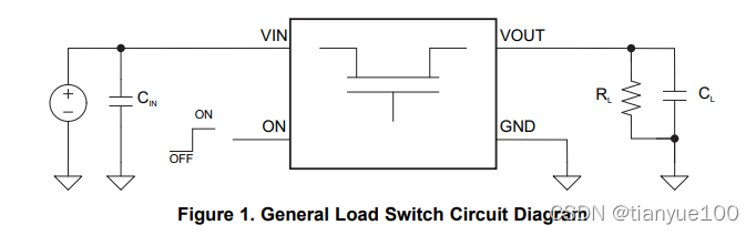
Integrated load switches are integrated electronic switches used to turn on and turn off power rails. Basic load switches consist of four pins: input voltage, output voltage, enable and ground. When the device is enabled via the ON pin, the pass FET turns on, thereby allowing current to flow from the input pin to the output pin, and power is passed to the downstream circuitry.
1.1 General Load Switch Block Diagram
An understanding of what the architecture of a load switch looks like will be helpful in determining the specifications of a load switch. Shown in Figure 2 is a block diagram of a basic load switch, which is made up of five basic blocks. Additional blocks can be included to add functionality to the load switch.

1. The pass FET is the main component of the load switch, which determines the maximum input voltage and maximum load current the load switch can handle. The on-resistance of the load switch is a characteristic of the pass FET and will be used in calculating the power dissipated by the load switch. The pass FET can be either an N-channel or P-channel FET, which will determine the architecture of the load switch.
2. The gate driver charges and discharges the gate of the FET in a controlled manner, thereby controlling the rise time of the device.
3. The control logic is driven by an external logic signal. It controls the turn-on and turn-off of the pass FET and other blocks, such as quick output discharge, the charge pump, and blocks with protection features. This external logic signal is commonly connected directly to an external microcontroller.
4. The charge pump is not included in all load switches. This is used in load switches with an N-channel FET, since a positive differential voltage between the gate and the source (VOUT) is needed in order to turn on the FET properly.
5. Quick output discharge is an on-chip resistor from VOUT to GND that is turned on when the device is disabled via the ON pin. This will discharge the output node, preventing the output from floating. For the devices with quick output discharge, this feature is only present when VIN and VBIAS are within the operating range.
6. Additional features are included in different load switches. These include, but are not limited to, thermal shutdown, current limiting, and reverse current protection.
1.2 Datasheet Parameters
Below is a list of common datasheet parameters and definitions for load switches.
• Input voltage range (VIN) – This is the range of input voltages that the load switch can support.
• Bias voltage range (VBIAS) – This is the range of bias voltages that the load switch can support. This may be required to power the internal blocks of the load switch, depending on the architecture of the load switch.
• Maximum continuous current (IMAX) – This is the maximum continuous DC current the load switch can support. System thermal performance plays a key role in determining the maximum continuous DC current in a system.
• ON-state resistance (RON) – This is the resistance measured from the VIN pin to the VOUT pin, which takes into consideration the resistance of the packaging and the internal pass FET.
• Quiescent Current (IQ) – This is the required amount of current to power the internal blocks of the device, which is measured as the current flowing into the VIN pin without any load on VOUT.
• Shutdown Current (ISD) – This is the amount of current flowing into VIN when the device is disabled.
• ON pin input leakage current (ION) – This is the amount of current that is flowing into the ON pin when the ON pin has a high voltage applied to it.
• Pull-down resistance (RPD) – This is the value of the pull-down resistor from VOUT to GND when the device is disabled.
2 Why Do You Need Load Switches
This section will provide a general overview of some applications where using a load switch is beneficial.
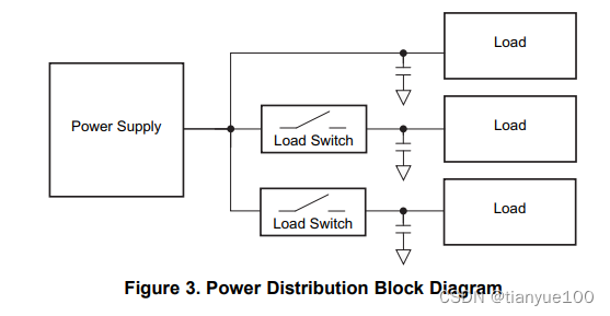
2.1 Power Distribution
Many systems have limited control of sub-systems power distribution. As iillustrated in Figure 3, load switches can be used to turn on and off sub-systems of the same input voltage instead of using multiple DC/DC converters or LDO’s. By using a load switch, power can be distributed across different loads with control for each individual load.
2.2 Power Sequencing and Power State Transition
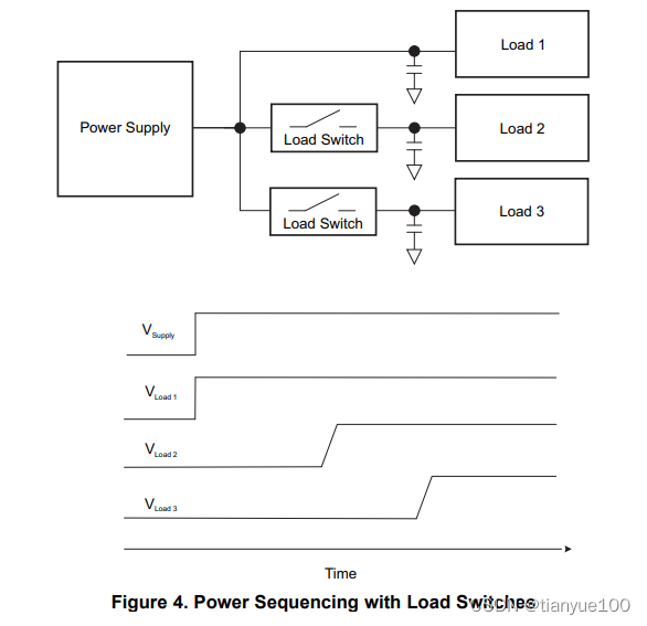
In some systems, especially those with a processor, there is a strict power-up sequence that must be followed. By using a GPIO or I 2C interface, load switches are a simple solution to implement power sequencing to meet the power-up requirements. Load switches can provide independent control of each power path to provide simplified point-of-load control for power sequencing, as shown in Figure 4.
2.3 Reduced Leakage Current
In many designs, there are sub-systems that are only used during certain modes of operation. Load switches can be used to limit the amount of leakage current and power consumption by turning off power to these sub-systems. Figure 5 shows a comparison of the leakage current with and without a load switch. Refer to the Input and Output Capacitance section for more details.
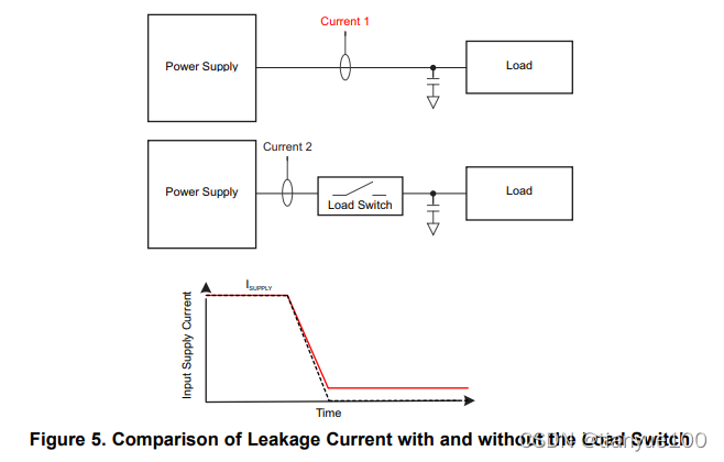
In some applications, the circuitry such as DC/DC converters, LDOs, and modules can be disabled and put into standby mode. However, the leakage current of these modules can be relatively high, even in the shutdown state. By placing a load switch before the load, as shown above, the leakage can be reduced to significantly lower levels. Thus, power consumption can be reduced significantly with a load switch placed in the power path.
2.4 Inrush Current Control
When turning on a sub-system without any slew rate control, the input rail may sag because of the inrush current that can happen from quickly charging a load capacitor. This can be problematic as this rail may be supplying power to other sub-systems (Figure 6). Load switches solve this issue by controlling the rise time of the output voltage, thereby eliminating the sag on the input voltage (Figure 7). The inrush current is proportional to the load capacitance as will be explained later in the Section 4.2 section.

2.5 Controlled Power Down
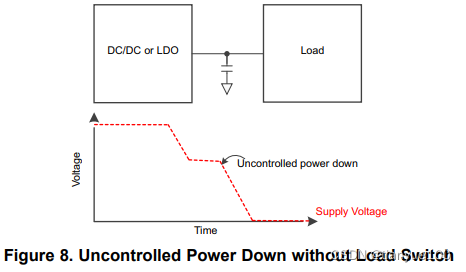
When a DC/DC converter or LDO without quick output discharge turns off, the load voltage is left floating and power down timing is dictated by the load, as shown in Figure 8. This can cause unwanted activity as modules downstream are not powered down to a defined state.
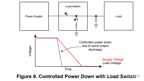
Using a load switch with quick output discharge can mitigate these problems. The load will be powered down quickly in a controlled manner and will be reset to a known good state for the next power up, as shown in Figure 9. This will eliminate any floating voltages at the input of the load and ensure that the load remains in a defined power state at all times.Refer to the Quick Output Discharge (QOD) section for more details.
2.6 Protection Features
Certain applications may require fault protection features to be integrated into the load switch. Some load switches include integrated features such as reverse current protection, ON pin hysteresis, current limiting, undervoltage lock-out and over temperature protection. Instead of implementing these complex circuits through discrete components, using an integrated load switch reduces BOM count, solution size, and development time. The list below briefly explains what some of these features can be:
• Reverse current protection will stop current from flowing from the VOUT pin to the VIN pin. In the absence of this feature, current may flow from the VOUT pin to the VIN pin!~, if the voltage on VOUT is greater than VIN by a diode drop. Thus, reverse current blocking may be beneficial in certain applications, such as in a power mux application where current should not flow from VOUT to VIN. There are many different methods of implementing reverse current protection. In some situations, such as the TPS22916, the device will monitor the voltage levels at the VIN pin and VOUT pin. When this differential voltage exceeds a certain threshold, the switch is disabled and the body diode is disengaged to prevent any reverse current flow to VIN. Some devices, such as the TPS22963C, only have reverse current protection when the device is disabled.
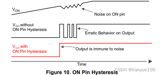
• ON pin hysteresis allows for more robust GPIO enable. With a voltage difference between a logic level high and logic level low on the ON pin, the control circuitry will operate as intended when there is noise on the GPIO line. Figure 10 illustrates how ON pin hysteresis can provide robustness on the GPIO enable line.
• Current limiting is a feature that will limit the amount of current the load switch will output. This will ensure that there is not an excessive amount of current being pulled by an external circuitry. If current is not limited, the external circuitry can potentially bring the main system down. In the current limited mode, load switch works as a constant current until the switch current falls below the current limit.
• Undervoltage lock-out (UVLO) is used to turn off the device if the VIN voltage drops below a threshold value, ensuring that the downstream circuitry is not damaged by being supplied by a voltage lower than intended.
• Over temperature protection disables the switch if the temperature of the device exceeds a threshold temperature. With this feature, the device can operate as a safety switch that turns off when a high temperature is detected.
2.7 Lower BOM Count and PCB Area
Using an integrated load switch can lower the BOM count of a system. If there are discrete FETs that are used in conjunction with other components, a load switch could be considered to reduce the number of total components in the system. When a load switch is created discretely, there are many resistors, capacitors and transistors that will be required to implement a gate driver, control logic, output discharge and protection features. With an integrated load switch, this is all accomplished with only a single device and the BOM count is significantly reduced.
3 Part Selection and Design Considerations
This section will look at the specifications that need to be kept in mind in choosing a load switch.
3.1 NMOS vs PMOS
In an NMOS device, the pass FET is turned on by bringing the gate voltage above the source. Usually, the source voltage is at the same potential as the VIN terminal. In order to create this voltage differential between the gate and the source, a charge pump is required. Using a charge pump will increase the quiescent current of the device.
In a PMOS device, the pass FET is turned on by bringing the gate voltage below the source voltage. The architecture of a PMOS device does not require a charge pump, resulting in a lower quiescent current when compared to a NMOS device.
One major difference between a PMOS based architecture and NMOS based architecture is that PMOS based load switches do not perform well at lower voltages, while NMOS devices are good for lower VIN applications.
3.2 ON-State Resistance (RON)
ON-state resistance (RON) is a particularly important specification, as this determines the voltage drop across the load switch and power dissipation of the load switch. The larger the RON, the larger the voltage drop across the load switch will be and the higher the power dissipation. Refer to Section 4 for calculations on how to determine the voltage drop and power dissipation.
3.3 Voltage (VIN) and Current (IMAX) Rating
One of the key considerations in selecting a load switch is the voltage and current required for the application. The load switch must be able to support the DC voltage and current that is expected during steady state operation, as well as the transient voltages and peak currents. It is important to note that some load switches require a bias voltage to turn on the device and bias the internal circuitry. This bias voltage is independent from the input voltage.
3.4 Shutdown Current (ISD) and Quiescent Current (IQ)
Quiescent current is the current that the load switch consumes when the load switch is ON. Quiescent current, in addition to the I 2R losses, will determine the amount of power that is consumed by the load switch when it is powered on. If the load currents are large enough, the power consumed due to quiescent current is negligible. Shutdown current determines the amount of power the load switch consumes when it is disabled via the ON pin. By using a load switch to power down subsystems, there can be a significant decrease in the standby power of a power rail. Refer to Section 5.2 for an example of how this may be an important specification.
3.5 Rise Time (tR )
Rise time varies from device to device. The rise time may need to be shorter or longer depending on the application. In addition to this, inrush current is inversely proportional to rise time. Knowing what inrush current is acceptable for the system can be beneficial. Refer to Section 4.2 for more details.
3.6 Quick Output Discharge (QOD)
Some load switches have an internal resistor that will pull the output to ground when the switch is turned off, preventing it from floating. For the quick output discharge feature to function, the voltage on the input voltage pins need within the operating range. There are many benefits to having the quick output discharge, such as:
• The output is not left floating and is always in a determined state.
• Downstream modules are always turned off completely. However, there are applications where quick output discharge would not be beneficial.
• If the output of the load switch was connected to a battery, quick output discharge would cause the battery to drain when the load switch is disabled via the ON pin.
• If two load switches are being used as a 2 input, 1 output multiplexer – where the outputs are tied together – the load switches cannot have quick output discharge. Otherwise, power would be constantly wasted through the quick output discharge, as current will be flowing through the internal resistor to ground whenever the load switch is disabled via the ON pin.
Load switches can offer the quick output discharge feature in either of these categories:
• Fixed quick output discharge. Devices with a fixed quick output discharge feature an internal, fixed resistor
• Adjustable quick output discharge. Devices such as TPS22918 have a dedicated pin that allows adjusting the discharge rate externally. • No quick output discharge at all.
3.7 Package Size
Integrated load switch come in all different shapes and sizes. Depending on the application, board space could be limited. In space constrained systems, it may be necessary to choose a smaller package size. For example, it may be undesirable to use 0.4 mm pitch devices. Thus, package size should be taken into consideration when deciding which device to choose.
3.8 Input and Output Capacitance
In load switch applications, input capacitors should be placed to limit the amount of voltage drop on the input supply caused by the transient inrush currents into the discharged load capacitors. A 1-µF capacitor between VIN and GND placed near the VIN terminal (CIN) is highly recommended. Higher values of capacitance will reduce the voltage drop during high-current applications. While this is highly recommended, it is not necessary for the load switch to operate.
The total output capacitance (CL ) between VOUT and GND may cause the voltage on VOUT to exceed the voltage on VIN when the supply is removed, which may result in current flow from VOUT to VIN through the body diode in the pass FET for devices without reverse current protection. It is recommended, but not required, to maintain a 10 to 1 ratio between the input capacitor and the load capacitance to prevent this.
4 Basic Calculations
This section has calculations that can be used to determine the specifications required for the load switch.
4.1 Voltage Drop
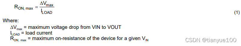
To determine an appropriate device for an application, it is necessary to understand how much voltage drop across the load switch is acceptable. The lower the acceptable drop, the lower the RON of the load switch must be. Use Equation 1 to determine the VIN to VOUT voltage drop:
4.2 Inrush Current

The value of the inrush current is determined by the total capacitance on VOUT and the rate of change of the VOUT voltage. Thus, it is important to ensure that the rise time of the load switch is chosen such that the device to exceed the maximum specifications – specifically IPLS – upon startup as indicated in the datasheet. Some devices have a separate CT pin, which allows the rise time to be programmed with an external capacitor from the CT pin to GND.
4.3 Power Dissipation
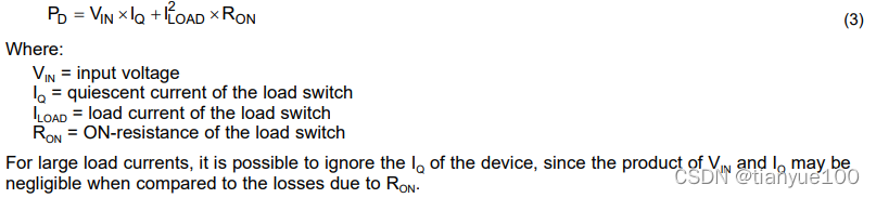
The input voltage and load current is necessary to calculate the power dissipated in the load switch. Use Equation 3 to determine the power dissipation of the load switch:
4.4 Thermal Considerations
The maximum IC junction temperature should be restricted to the maximum junction temperature as indicated on the absolute maximum table under normal operating conditions. To calculate the maximum allowable power dissipation, PD(max) for a given output current and ambient temperature, use Equation 4:

5 Design Examples and Application Examples
This section will discuss several examples that utilize the equations that were discussed in the previous section and present a few configurations of how a load switch can be used in a system.
5.1 RON and Inrush Current Calculations
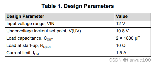
Listed below are the system specifications for this example:
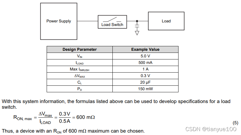

5.2 Standby Power Savings
For some battery operated systems, there is a power budget that must be met when operating in different modes. This section will illustrate the potential power savings with a load switch in the power path.
Some modules, such as LCD displays, power amplifiers, GPS modules, and processors, can have several mA or more of leakage current in their standby mode, but using a load switch can reduce this current to µA’s. For example, there is a 5 V rail with a downstream module that has 1 mA of leakage current, the power dissipated by this rail with the downstream module disabled is:
5 V × 1 mA = 5 mW
With a load switch in the system, the path that the leakage current is shunted to ground through the load switch and can be reduced to less than 1 µA. Thus, the power dissipated by this rail now becomes:
5 V × 1 µA = 5 µW
Thus, using a load switch will result in power savings by a factor of 1000. As the number of rails increase, placing additional load switches to reduce the power consumption of standby rails that have excessive leakage current can result in significant power savings.
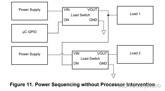
5.3 Power Sequencing without Processor Intervention
In the configuration shown in Figure 11, the load switches are arranged such that there is power-up sequencing without any processor intervention. In the diagram shown below, when the µC GPIO turns on the load switch, it will provide power to load 1. Once the voltage rail of load 1 has exceeded the VIH level of the second load switch, the second load switch will turn on. While the diagram below only shows one additional load switch is being enabled, this can be expanded to allow for one GPIO line to sequence many load switches. For more information, consider looking at Power Sequencing Reference Design using Load Switches.
5.4 2-to-1 Power Mux
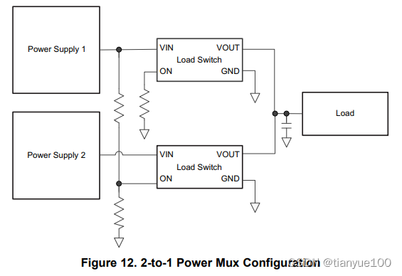
In the following configuration (Figure 12), two active-low load switches with reverse current protection can be configured to multiplex two supplies to one load. Active-low load switches are devices that turn on when the ON pin is pulled low. As shown in the following figure, this configuration gives priority to Power Supply 1. Whenever Power Supply 1 has a voltage applied, the load switch on the bottom gets disabled due to the resistor divider. The load switch connected to Power Supply 1 is kept on, but reverse current protection will prevent current from flowing from VOUT to VIN. Without external resistors, a microcontroller GPIO can drive the individual ON pins of the load switches. For more information, consider reading Power Multiplexing Using Load Switches and eFuses.
6 Conclusion
Integrated load switches are an effective solution for achieving power sequencing, power distribution, controlled rise time, lower standby power, lower BOM count, and smaller PCB area. As shown in this application note, a load switch from the TPS229xx and TPS2281x family can be easily integrated into any system with a few simple calculations to lower power consumption and simplify power supply design.
7 References
For more details on any of the concepts described in this document, refer to the following documents:
1. Integrated Load Switches versus Discrete MOSFETs (SLVA716)
2. Managing Inrush Current (SLVUA74)
3. Load Switch Thermal Considerations (SLVUA74)
4. Quiescent Current vs Shutdown Current for Load Switch Power Consumption (SLVA757)
5. Reverse Current Protection in Load Switches (SLVA730)
6. Fundamentals of On-Resistance in Load Switches (SLVA771)
7. Timing of Load Switches (SLVA883)
8. Power Multiplexing Using Load Switches and eFuses (SLVA811) For additional information, refer to Load Switches.
Power Multiplexing Using Load Switches and eFuses
Power Multiplexing Using Load Switches and eFuses
https://www.ti.com/lit/an/slva811a/slva811a.pdf?ts=1649477278097
eFuse: Safety Certification and why it Matters
11 Ways to Protect Your Power Path white paper
How to use load switches and eFuses in your set-top box design
Why bother turning different loads on and off?
STB designers usually follow standby power requirements so they can improve the system’s power efficiency. These requirements limit the amount of power that the STB can draw when it is inactive, so different subsystems need to be off in order to draw a minimal amount of power. Some regions even have specific power requirements, such as such as Energy Star. Figure 2 shows the common STB subsystems that can be controlled to improve standby power.
Figure 2: Load switch and eFuse applications in STBs
Now let’s take a look at some of the subsystems you can switch on and off.
- Front end/tuner. This subsystem takes the input signal (cable or satellite) and converts the signal into video. One tuner is responsible for a single video output, so if an STB can record five shows at once, that means that there are five different tuners dedicated to recording. Likewise, there is a tuner for the output video port and for connecting additional devices through Wi-Fi®. Switching the tuners off when they are not being used can reduce shutdown power.
- Hard drive. A hard drive that is not recording a show or playing a previously recorded show does not need to be active. This is also the case when the STB is just outputting the cable signal.
- Wi-Fi. Wi-Fi connects additional devices to the STB such as tablets or computers, or connects smaller STBs within the same household.
Load switches can control power to each of these subsystems, and both the TPS22918 and TPS22975 can be used depending on the current load. Both are plastic devices that come with an adjustable output rise time suitable for different capacitive loads. The TPS22918 can support loads up to 2A and the TPS22975 can support loads up to 6A.
What about using switches for additional features?
Aside from power savings, several other features require a switch:
- Power sequencing. The system on chip (SoC) or microcontroller that controls the STB has a specific power-on sequence for its different voltage rails. For optimal performance, devices like the TPS22918 or TPS22975 can turn on each of the rails in order.
- Input protection. Voltage and current transients can occur when the 12V adapter is plugged into the STB. Placing the TPS2595 eFuse at the STB input can protect the rest of the system from hot-plug events.
- SD card. If an STB uses an SD card, the option exists to power it with 3.3V or 1.8V. Using the TPS22910A and TPS22912C load switches enables you to choose the appropriate rail.
- HDMI. The HDMI port is powered with 5V when in use, and the current needs to be limited for user protection. The TPS22945 load switch has a low current limit of 100mA.
All of these applications are modeled in the block diagram in Figure 3.
Figure 3: Recommended load switches and eFuses in STBs
Where can you get started?
The Power Switching Reference Design for Set Top Box shows all of the different load switches and eFuses used for each subsystem. With the added DC/DCs, the design helps create a complete solution for STB power delivery.
Figure 4: Power Switching Reference Design for Set Top Box
With the trend in STB moving to smaller form factors, it’s easy to see why designers are looking for more integration in their systems. So keep your STB power design small and easy, and use load switches and eFuses to accomplish your varying power switching needs!
Additional resources
- Only have a few minutes? Watch some videos:
- “Load Switches vs. Discrete MOSFETs” (2:35).
- “Load Switches vs. Discrete MOSFETs – Problems with a discrete solution and how a load switch can fix them” (3:22).
- Learn more about load switches by downloading these application notes:
- “Basics of Load Switches.”
- “Integrated Load Switches versus Discrete MOSFETs.”
- Check out the following load switch blog post for more information:
How can a load switch extend your device’s battery life?
Let’s say that you’re a power electronics engineer and your boss has asked you to extend the battery life of your product. After optimizing the front-end power path (battery charger) and mid-rail converters (DC/DCs and low-dropout regulators [LDOs]), you believe there’s no room left to squeeze out a few more hours or days of battery life. You’re almost ready to report back that it’s impossible, but after taking a look in your toolbox, you find the solution: load switches.
One of the many ways that you can use a load switch is to reduce the shutdown current of any load. Do you have a Bluetooth® or Wi-Fi® module that consumes over 10µA in deep sleep or hibernation mode? Try adding a load switch like the TPS22916 in Figure 1, which can reduce the shutdown current to just 10nA.

Figure 1: Reduce shutdown current by adding a low-leakage load switch between the supply and load.
In some applications, such as wearables, building automation or medical devices, there can be several sensors and wireless transmitters in a single product that load switches can disable. Figure 2 shows the system block diagram of a typical smartwatch and where load switches would be used in the power path.
Figure 2: Smartwatch system block diagram
Take an example of a smartwatch using a standard 3.7V lithium polymer battery with 65mAh of capacity. In order to last at least five days before charging (a typical work week), you need to leave certain sensors powered (like the step counter), but you can shut down other areas of the board, like the Bluetooth® module. If the Bluetooth® module draws 10µA when disabled, it is contributing to at least 10µA × 24 hours × 5 days = 1.2mAh of the 65mAh budget. In other words, this one module is contributing at least 1.8% (1.2mAh/65mAh) to overall battery-life loss. Plus, this very conservative estimate does not take into account minimum/maximum specs over temperature, nor efficiency loss through the DC/DC converters. If you have several modules leaking current, the situation can multiply very quickly.
How do you combat this? Using the TPS22916 will cut that shutdown leakage current to just 10nA. This means that you can continue using your favorite Bluetooth module and it will have virtually no effect (0.0018%) on battery life when disabled, thanks to your new favorite load switch.
To learn more about load switches and the features they can offer, be sure to check out ti.com/loadswitch.


 1500
1500


 被折叠的 条评论
为什么被折叠?
被折叠的 条评论
为什么被折叠?
 到【灌水乐园】发言


