


1 Input Capacitor Selection
1.1 Reduce Input Ripple Voltage
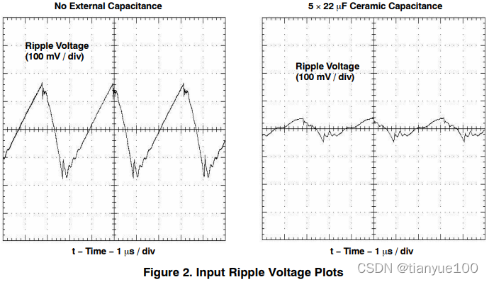
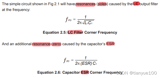
The first objective in selecting input capacitors is to reduce the ripple voltage amplitude seen at the input of the module. This reduces the rms ripple current to a level which can be handled by bulk capacitors.
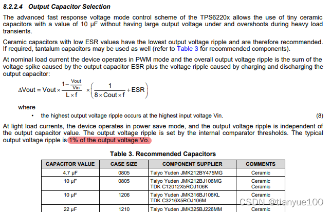
Ceramic capacitors placed right at the input of the regulator reduce ripple voltage amplitude. Only ceramics have the extremely low ESR that is needed to reduce the ripple voltage amplitude. These capacitors must be placed close to the regulator input pins to be effective. Even a few nanohenries of stray inductance in the capacitor current path raises the impedance at the switching frequency to levels that negate their effectiveness.
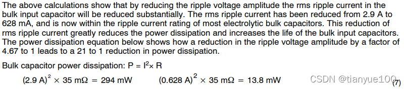
Large bulk capacitors do not reduce ripple voltage. The ESR of aluminum electrolytics and most tantalums are too high to allow for effective ripple reduction. Large input ripple voltage can cause large amounts of ripple current to flow in the bulk capacitors, causing excessive power dissipation in the ESR parasitic.
To reduce the rms current in the bulk capacitors the ripple voltage amplitude must be reduced using ceramic capacitors. As a general rule of thumb, keeping the peak to peak ripple amplitude below 75 mV keeps the rms currents in the bulk capacitors within acceptable limits.
1.2 Selecting Input Ceramic Capacitors
Load current, duty cycle, and switching frequency are several factors which determine the magnitude of the input ripple voltage.
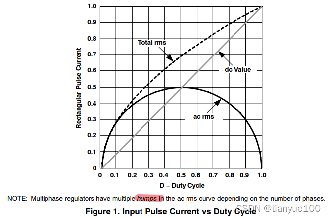
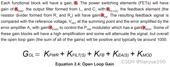
The input ripple voltage amplitude is directly proportional to the output load current. The maximum input ripple amplitude occurs at maximum output load. Also, the amplitude of the voltage ripple varies with the duty cycle of the converter. For a single phase buck regulator, the duty cycle is approximately the ratio of output to input dc voltage. A single phase buck regulator reaches its maximum ripple at 50% duty cycle. Figure 1 shows the ac rms, dc, and total rms input current vs duty cycle for a single phase buck regulator. The solid curve shows the ac rms ripple amplitude. It reaches a maximum at 50% duty cycle. The chart shows how this magnitude falls off on either side of 50%. The straight solid line shows the average value or dc component as a function of duty cycle. The curved dashed line shows the total rms current, both dc and ac, of the rectangular pulse as duty cycle varies.
1.3 Calculating Ceramic Capacitance
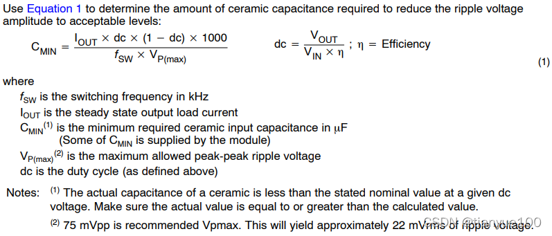
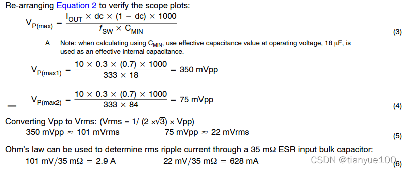
A Note: when calculating using CMIN, use effective capacitance value at operating voltage, 18 μF, is used as an effective internal capacitance.
1.4 Input Inductor
If reflected ripple is a concern, use a small (560 nH or less) input inductor. This is the single most effective way to confine ripple currents to the local input bypass caps. An input inductor can reduce the reflected ripple current by an order of magnitude. A single input inductor can be shared by multiple modules.
At lower currents, this input inductor can take the form of a power ferrite bead. In a multiple module system, the use of a filter inductor at each module will help contain the noise generated by each module and keep it localized. It is one of the best ways to deal with beat frequencies caused by multiple modules operating at slightly different frequencies. Ensure the inductor current is below its saturation current rating.
During transient conditions, the use of an input inductor puts larger demands on input bulk capacitors. Take care when using input inductors as they will affect input capacitor selection.
1.5 Transients and Bulk Capacitors
When output current transients are involved the key point to keep in mind is that the electrons have to come from the input of the regulator. Bulk capacitors control the voltage deviation at the input when the converter is responding to an output load transient. The higher the capacitance, the lower the deviation. Therefore, the size of the input bulk capacitor is determined by the size of the output current transient and the allowable input voltage deviation.
The amplitude of the input voltage deviation during a transient is directly proportional to the load current change. If the magnitude of the transient load current is doubled, the input voltage disturbance is doubled also.
Lower input voltage means higher input currents. The input current scales directly by duty cycle. At lower input voltages the input transient currents will also be higher. To comply with output voltage deviation limits, more input capacitance is required.
Consider a 2.5 V output regulator with a 10 A transient load. With a 12 V input, the ideal duty cycle is 2.5 / 12 = 0.208. The 10 A load transient on the output transforms to a 2.08 A transient on the input. With a 3.3 V input regulator, the duty cycle is now 2.5 / 3.3 = 0.758. The 10 A load transient is now a 7.58 A input transient. This will cause a larger voltage deviation on the lower voltage supply where the voltage limits are probably tighter.
During a transient, input inductance slows the current slew rate seen by the host supply. The use of a filter inductor places more demands on the input bulk capacitors since more of the initial current demand must come from the input capacitors rather than the host supply. The input voltage at the regulator input now sees a much higher voltage deviation. In the end, both the input and output capacitors have to be recharged, causing higher peak currents to be demanded from the host supply.
Note: Be careful when using the input inductor
1.6 Example Bulk Capacitor Calculation
When designing a system consisting of a single POL module, or multiple POL modules that make use of a shared bulk input capacitor bank, the first step is to calculate the magnitude of the input transient current. This is done by calculating the reflected input transient for each POL module’s output transient.
After calculating the individual input transients for each module, add them up to get the total transient current. When calculating, you must determine the worst case transient combination of all modules and proceed accordingly.
input current transient
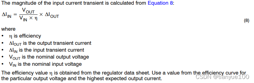
Figure 3 shows an example diagram of multiple POL modules sharing a single bank of bulk input capacitors. The output voltage, output current and output load transient specifications are given. The input transient current is calculated for each POL. Adding the individual input transients, the total calculated input transient current is 2.774 A.
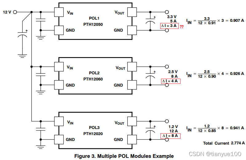
Think about how to get the value of Delta_I_load in equation above???
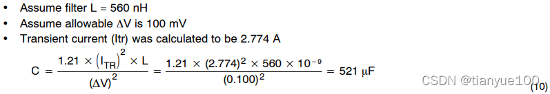
The next step is to decide if a series filter inductor is going to be used. If using an inductor, pick a value no greater than 560 nH. If not using one, use a value of 50 nH in the calculation to account for stray inductance in the host supply path and its finite bandwidth.
Next, determine the maximum allowable voltage deviation on the bulk capacitors. This is the maximum allowable dip during the peak transient step that was calculated in step one. The smaller the voltage deviation, the higher the required amount of bulk capacitance.
1.6.1 Calculation
Think about how to get the value 1.21 in equation above ???
According to the calculation we need 521 μF of bulk capacitance at a minimum. We would use the nearest standard value of 560 μF.
Use low ESR capacitors to implement the bulk network. Capacitors with high ESR induce voltage drops of their own due to the current flowing in them.
Care must be taken when using very low ESR capacitors together with an input inductor as it may cause instability. Always use an oscilloscope to monitor the input voltage to the POLs during transient testing to insure that you have a stable system.
2 Output Capacitor Selection
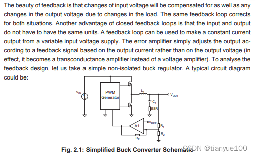
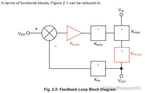
2.1 Output Capacitors Effect Feedback
The output capacitance of a switching regulator is a vital part of the overall feedback system. The energy storage inductor and the output capacitor form a second-order low-pass filter.
As the output voltage is sensed across both the filter and load impedance, they both affect the feedback control loop. Adding external capacitance shifts the corner frequency of this filter. The external component parameters, including capacitor impedance, are part of the feedback control loop.
The impedance of the output capacitance affects the damping of the output filter and has a major affect on the transient response of the supply.
In general, low-ESR capacitors are good choices. They provide excellent energy storage and improve the transient performance. However, if the overall impedance of the output capacitor network is too low, the dynamic response of the regulator can be adversely affected.
To understand how output capacitor impedance affects the stability of the feedback loop, it helps to understand the impedance characteristics of various capacitor types.
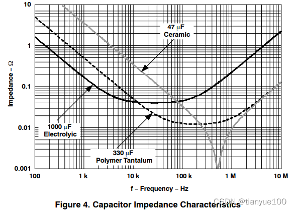
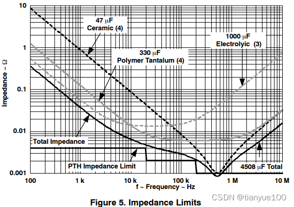
Figure 4 shows the impedance characteristics for three common capacitor types; electrolytic, polymer tantalum, and multi-layer ceramic. Each capacitor type is characterized by its impedance and the frequency range over which it is most effective. The frequency at which the impedance reaches its minimum is determined by its ESR and ESL. It is known as the self resonant frequency of the capacitor.
The self resonant frequency is considered to be the maximum usable frequency for a capacitor. Above this frequency the impedance of the capacitor begins to rise as the ESL of the capacitor begins to dominate. Note that each capacitor type has a specific frequency band over which it is most effective. Therefore, a capacitor network of multiple capacitor types is more effective in reducing impedance than just one type.
For the PTH family of switching regulators the output capacitor impedance limits can be easily defined. For optimum performance, the overall impedance of the external output capacitor network must meet the following criteria:
- Must be greater than 4 mΩ for frequencies below 20 kHz.
- Must be greater than 2 mΩ for frequencies between 20 kHz and 200 kHz.
- Above 200 kHz the impedance can fall below 2 mΩ.
Figure 5 shows the impedance limit of the PTH modules. Also plotted is the total impedance curve for a capacitor network made up of electrolytics, polymer tantalums, and multi-layer ceramics. The capacitor network achieves low impedance without violating the impedance limits. Notice how each individual set of capacitors gets nowhere close to the impedance limit curve. Always take into account the impedance of all the capacitors in the network, as a combined network will always exhibit lower impedance than any one capacitor type.
If the output capacitor network’s impedance falls below the limit, the transient response will exhibit insufficient damping and may become unstable.
External output capacitors are required to achieve fast response to load transients. This is necessary to compensate for the both the parasitic resistance and inductance of the PCB traces. The capacitors internal to the module will have no effect at the remote load terminals at frequencies above 1 MHz. The parasitic resistance and inductance of the PCB traces decouple the regulator from its load. To insure good high frequency regulation at the point of load, local decoupling capacitors must be used.
There is no limit on the number of low-value (< 1 μF) ceramic capacitors that can be used. Low-value ceramic capacitors are only effective at frequencies above 1 MHz, well beyond the bandwidth of the feedback loop. As a result, they have only a minor impact on the regulator’s feedback control loop. They do, however, provide tremendous benefit when dealing with very fast load transients. For this reason these capacitors should be placed right at the IC’s that are generating the transients.
The resonant frequency of ceramic capacitors increases by a factor of 3.16 for every decade decrease in capacitance value. A 1 μF ceramic capacitor might have a usable frequency of 5 MHz, and a value of 0.1 μF might work up to 15 MHz. To handle frequencies above 100 MHz, bypass capacitors with values defined in pico-Farads(pF) must be used.
2.2 Importance of Output Capacitors
The current slew rate of a regulator is limited by its output filter inductor. When the amount of current required by the load changes, the initial current deficit must be supplied by the output capacitors until the regulator can meet the load demand.
Figure 6 shows a simplified buck regulator circuit as an example. When a load transient occurs, the regulator feedback control loop senses the change in output voltage and begins to change the power transistor duty to compensate. Even if the duty cycle is able to instantly rise to 100%, the rate in which the output current can change is limited by the value of the regulator’s output filter inductor.
The equation that governs this is: di/dt = ΔV/L.
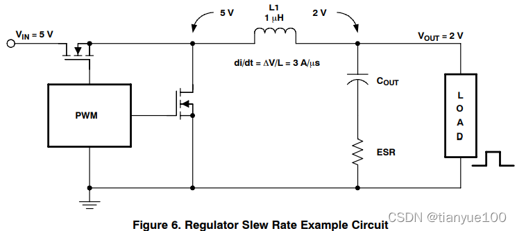
In the example circuit, Vin is 5 V and Vout is 2 V. At 100% duty there is 3 V across the 1μH inductor. The equation shows that the maximum rate of current change is 3 A/μs. This is the fastest rate at which the regulator output current can be increased. Until the regulator can increase the load current to the new value, the deficit must come from the output capacitors.
Capacitors all have some parasitic series resistance (ESR). Any current flowing in the capacitor must also flow through the ESR. This causes a voltage drop due to the I×ESR product. Each mΩ of resistance will cause 1 mV of voltage drop for every 1 A of output transient current.
For a very fast load transient of magnitude ΔI, the best case peak voltage deviation (ΔV) will be ΔI times the combined ESR of the output capacitors(=ΔI×ESR). The regulator has no influence over it. For slower transients, the regulator feedback loop will help reduce the peak voltage deviation.
2.3 Designing for Transient Performance
When designing for a load transient, the output bulk capacitors and high frequency bypass capacitors determine the response performance and voltage deviation of the regulator. The most important parameters are the magnitude of the load transient (ΔI) and the distributed bus impedance to the load. The selection of the output capacitors is determined by the allowable peak voltage deviation (ΔV). This limit should reflect the actual requirements, and should not be specified lower than needed.
The distribution bus impedance seen by the load is the parameter that determines the peak voltage deviation during a fast transient. The system requires a low impedance bus over all frequencies with adequate bypass capacitors to achieve fast slew rates. If the impedance of the network that supplies the load remains below a maximum impedance, the voltage deviation due to the transient will remain within allowable voltage deviation requirements. It is simply Ohm's Law: ΔV = ΔI × Z. Keep the magnitude of Z below the maximum limit, and the transient voltage deviation will stay within its limits.
Divide ΔV by the ΔI to determine the maximum allowable impedance, Zmax. This is the impedance limit which must be maintained by the output capacitor network for frequencies above which the regulator is effective.
To maintain low impedance from the regulator to the load, high frequency, low value ceramic capacitors must be placed very close to the load to minimize the effects of trace inductance while larger value ceramic capacitors can be placed closer to the regulator.
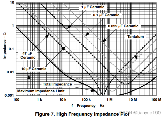
In Figure 7 the impedance of an output capacitor network is shown. At the lower frequencies (≤ 10 kHz), the regulator’s feedback loop will keep the output impedance low. As the regulator’s gain falls off, its output impedance will rise. External output capacitors are now required to keep the impedance low over the higher frequency range. As can be seen, multiple low value ceramic capacitors are required to keep the impedance low at very high frequencies. No single value of capacitance can cover the entire frequency range. Internal parasitic inductance within a capacitor limits its maximum usable frequency. the lower the value of capacitance, the higher its usable frequency. To cover multiple decades of frequency, you must use multiple decades of capacitance values.
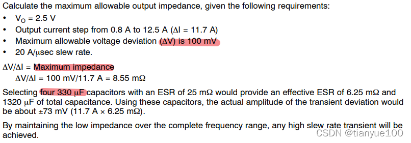
2.4 Transient Design Example
2.5 Absolute Maximum Capacitor Limits
All regulators have an absolute maximum capacitance limit.
Many modules incorporate output short-circuit protection. During startup, the regulator must charge the output capacitance in order to raise the output voltage to its set-point. This limits how much capacitance can be added.
Startup behavior is triggered by:
- • the application of power
- • the removal of a ground signal from the Inhibit pin
- • the regulator’s recovery from an over-current condition
Any of these instances result in the regulator’s output voltage rising rapidly from zero up to its set-point. When the output voltage rises, current flows to the capacitance according to the equation: I = C dV/dt, where dV/dt is the slew rate of the output voltage.
The output voltage slew rate during the regulator’s startup is approximately 1 V/msec for most PTH products. This causes 1 A of current to flow to the output capacitance per 1000 μF of capacitance value. This current is in addition to any load current that may be drawn by the application circuit.
If there is too much output capacitance, the current demanded from the regulator trips its over-current protection circuit. Furthermore, each over-current trip will be followed by further attempts by the regulator to restart. This can result in the regulator entering a perpetual cycle of over-current shut down.
2.6 In the Data sheet
Data sheet tables give the maximum allowable output capacitance for each module.
If external capacitance is required for stable operation, the minimum value will be listed in the datasheet. Recommended capacitance is also listed in the datasheet for improved transient performance. The recommended capacitance value will meet a typical ΔV spec at a 50% transient load step.
If the required ΔV is less than the recommended typical ΔV spec, or the transient load step is greater than 50%, more output capacitance must be added. In each case the maximum ESR required to meet your transient goal must be calculated.
See the Electrical Characteristics section in the PTH/PTV series data sheets.
2.7 Conclusion
In any power system, input and output capacitance is key to optimum performance. Good engineering practice requires that additional external capacitance be placed at the input and output of all regulators. A well designed power supply decoupling network will employ different types of capacitors. System design requirements will determine the amount and type of capacitors for any design.
Detailed analysis has been performed to allow capacitor limits to be accurately defined. By following the capacitor recommendations in the data sheet and selecting capacitors based on your actual operating conditions, a reliable, low-cost power system can be designed.
TPS6220x High-Efficiency, SOT23 Step-Down, DC-DC Converter datasheet (Rev. F)
ADP1874/ADP1875 (Rev. A)
https://www.analog.com/media/en/technical-documentation/data-sheets/ADP1874_1875.pdf
OUTPUT CAPACITOR SELECTION
The primary objective of the output capacitor is to facilitate the reduction of the output voltage ripple; however, the output capacitor also assists in the output voltage recovery during load transient events. For a given load current step, the output voltage ripple generated during this step event is inversely proportional to the value chosen for the output capacitor. The speed at which the output voltage settles during this recovery period depends on where the crossover frequency (loop bandwidth) is set. This crossover frequency is determined by the output capacitor, the equivalent series resistance (ESR) of the capacitor, and the compensation network.
To calculate the small signal voltage ripple (output ripple voltage) at the steady state operating point, use the following equation:
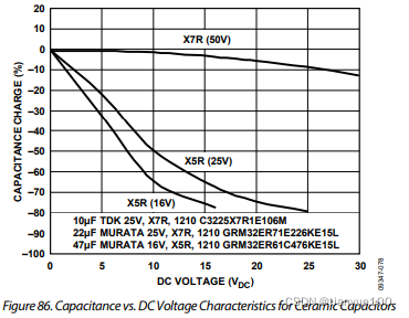
Ceramic capacitors are known to have low ESR. However, there is a trade-off in using the popular X5R capacitor technology because up to 80% of its capacitance may be lost due to derating as the voltage applied across the capacitor is increased (see Figure 86). Although X7R series capacitors can also be used, the available selection is limited to 22 µF maximum.
Electrolytic capacitors satisfy the bulk capacitance requirements for most high current applications. However, because the ESR of electrolytic capacitors is much higher than that of ceramic capacitors, several MLCCs should be mounted in parallel with the electrolytic capacitors to reduce the overall series resistance.
INPUT CAPACITOR SELECTION
The goal in selecting an input capacitor is to reduce or minimize input voltage ripple and to reduce the high frequency source impedance, which is essential for achieving predictable loop stability and transient performance.
The problem with using bulk capacitors, other than their physical geometries, is their large equivalent series resistance (ESR) and large equivalent series inductance (ESL). Aluminum electrolytic capacitors have such high ESR that they cause undesired input voltage ripple magnitudes and are generally not effective at high switching frequencies.
If bulk electrolytic capacitors are used, it is recommended to use multilayered ceramic capacitors (MLCC) in parallel due to their low ESR values. This dramatically reduces the input voltage ripple amplitude as long as the MLCCs are mounted directly across the drain of the upper side MOSFET and the source terminal of the lower side MOSFET (see the Layout Considerations section). Improper placement and mounting of these MLCCs may cancel their effectiveness due to stray inductance and an increase in trace impedance.
The maximum input voltage ripple and maximum input capacitor rms current occur at the end of the duration of 1 − D while the upper side MOSFET is in the off state. The input capacitor rms current reaches its maximum at Time D. When calculating the maximum input voltage ripple, account for the ESR of the input capacitor as follows:
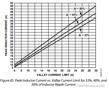
INDUCTOR SELECTION
When selecting the inductor, choose an inductor saturation rating that is above the peak current level, and then calculate the inductor current ripple (see the Valley Current-Limit Setting section and Figure 85).
DESIGN EXAMPLE
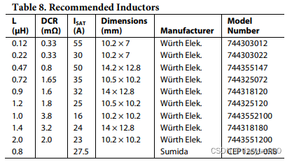
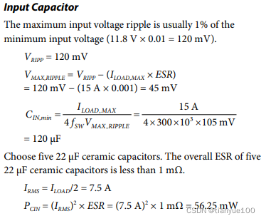
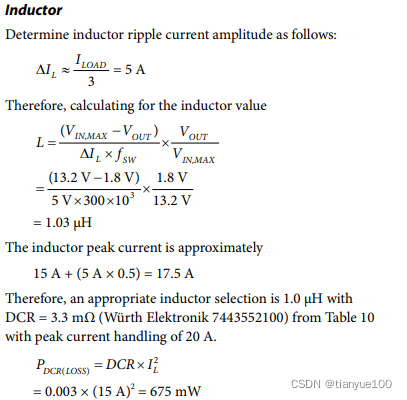
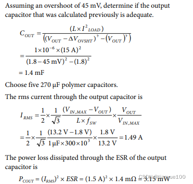
The ADP1874/ADP1875 are easy to use, requiring only a few design criteria. For example, the example outlined in this section uses only four design criteria: VOUT = 1.8 V, ILOAD = 15 A (pulsing), VIN = 12 V (typical), and fSW = 300 kHz.
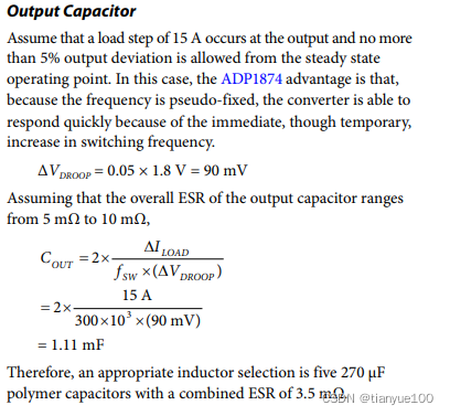
Others Reference:
DC_DC_Book_of_Knowledge.pdf
https://media.digikey.com/pdf/Data%20Sheets/Recom%20Power%20Inc%20PDFs/DC_DC_Book_of_Knowledge.pdf

Initial Evaluation of a DC/DC Switch Mode Power Supply Application Note
The R&S®RTO-K31 Power Analysis option supports setup, execution, viewing test results, and documentation. In the following, the power-on behavior will be evaluated, using the “Inrush Current” measurement function of the K31 option. ‘One-shot’ documentation of the primary parameters-ofinterest in the DC/DC converter start-up is achieved with the following additional channel selections and adjustments.
Input Filter Design for Switching Power Supplies
Input Filter Design for Switching Power Supplies https://www.ti.com/lit/an/snva538/snva538.pdf
Switching regulator fundamentals
2.2 Continuous vs Discontinuous Operation
In most Buck regulator applications, the inductor current never drops to zero during full-load operation (this is defined as continuous mode operation). Overall performance is usually better using continuous mode, and it allows maximum output power to be obtained from a given input voltage and switch current rating.
In applications where the maximum load current is fairly low, it can be advantageous to design for discontinuous mode operation. In these cases, operating in discontinuous mode can result in a smaller overall converter size (because a smaller inductor can be used).
Discontinuous mode operation at lower load current values is generally harmless, and even converters designed for continuous mode operation at full load will become discontinuous as the load current is decreased (usually causing no problems).
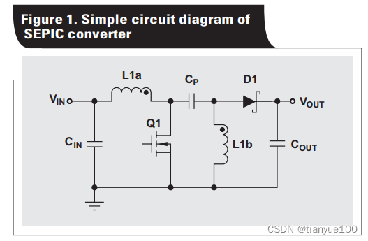
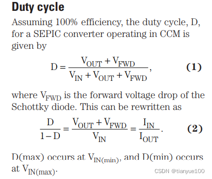
Designing DC/DC converters based on SEPIC topology
Designing DC/DC converters based on SEPIC topology (ti.com)
The single-ended primary-inductance converter (SEPIC)
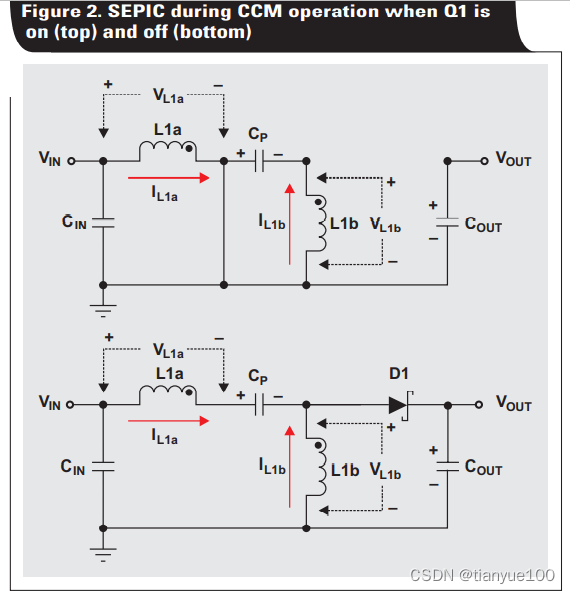
Selecting passive components One of the first steps in designing any PWM switching regulator is to decide how much inductor ripple current, ∆IL, to allow. Too much increases EMI, while too little may result in unstable PWM operation. A rule of thumb is to use 20 to 40% of the input current, as computed with the power-balance equation,

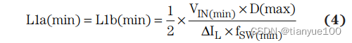
In this equation, IIN from Equation 2 is divided by the estimated worst-case efficiency, η, at VIN(min) and IOUT(max) for a more accurate estimate of the input current, IIN′. In an ideal, tightly coupled inductor, with each inductor having the same number of windings on a single core, the mutual inductance forces the ripple current to be split equally between the two coupled inductors. In a real coupled inductor, the inductors do not have equal inductance and the ripple currents will not be exactly equal. Regardless, for a desired ripple-current value, the inductance required in a coupled inductor is estimated to be half of what would be needed if there were two separate inductors, as shown in Equation 4:
To account for load transients, the coupled inductor’s saturation current rating needs to be at least 20% higher than the steady-state peak current in the high-side inductor, as computed in Equation 5:

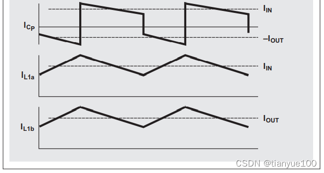
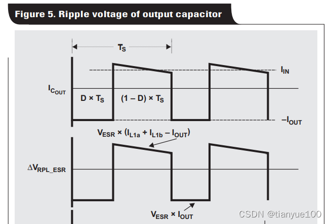
Note that IL1b(Peak) = IOUT + ∆IL /2, which is less than IL1a(Peak).
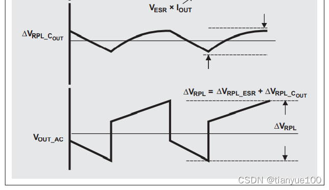
Figure 5 breaks down the capacitor ripple voltage as related to the output-capacitor current. When Q1 is on, the output capacitor must provide the load current. Therefore, the output capacitor must have at least enough tance, but not too much ESR, to meet the application’s requirement for output voltage ripple, ∆VRPL:
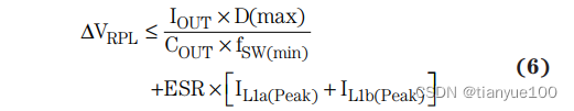
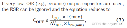
where fSW(min) is the minimum switching frequency. A minimum capacitance limit may be necessary to meet the application’s load-transient requirement.
The output capacitor must have an RMS current rating greater than the capacitor’s RMS current, as computed in Equation 8:

The input capacitor sees fairly low ripple currents due to the input inductor. Like a boost converter, the input current waveform is continuous and triangular; therefore, the input capacitor needs the RMS current rating,

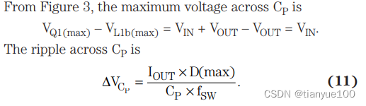
The coupling capacitor, CP, sees large RMS current relative to the output power:

Selecting active components
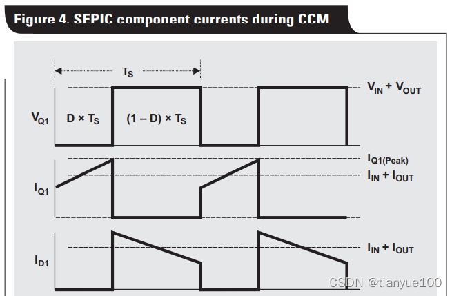
The power MOSFET, Q1, must be carefully selected so that it can handle the peak voltage and currents while minimizing power-dissipation losses. The power FET’s current rating (or current limit for a converter with an integrated FET) will determine the SEPIC converter’s maximum output current.
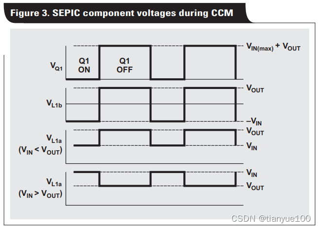
As shown in Figure 3, Q1 sees a maximum voltage of VIN(max) + VOUT. As shown in Figure 4, Q1 must have a peak-current rating of
![]()
At the ambient temperature of interest, the FET’s power dissipation rating must be greater than the sum of the conductive losses (a function of the FET’s rDS[on]) and the switching losses (a function of the FET’s gate charge) as given in Equation 13:
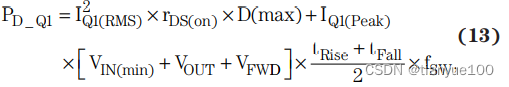
where tRise is the rise time on the gate of Q1 and can be computed as Q1’s gate-to-drain charge, QGD, divided by the converter’s gate-drive current, IDRV. Q1’s RMS current is

The output diode must be able to handle the same peak current as Q1, IQ1(Peak). The diode must also be able to withstand a reverse voltage greater than Q1’s maximum voltage (VIN[max] + VOUT + VFWD) to account for transients and ringing. Since the average diode current is the output current, the diode’s package must be capable of dissipating up to PD_D1 = IOUT × VFWD.


 1088
1088

 被折叠的 条评论
为什么被折叠?
被折叠的 条评论
为什么被折叠?
 到【灌水乐园】发言


