


一
1、用Logsim绘制一个3-8译码器电路图
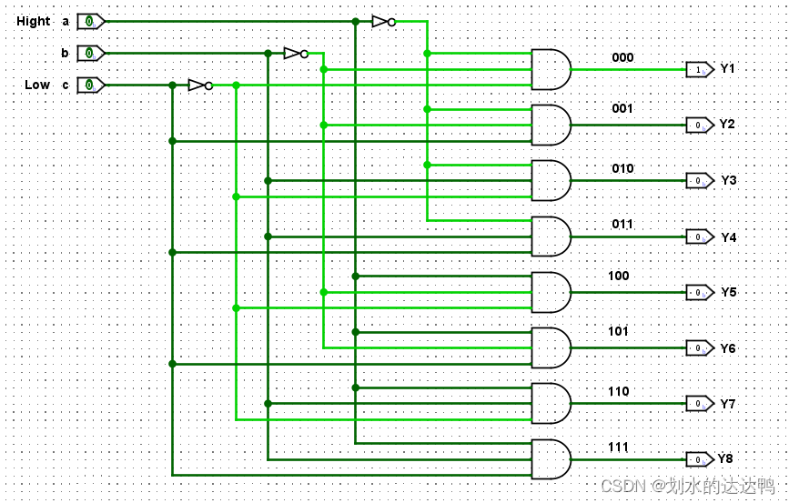
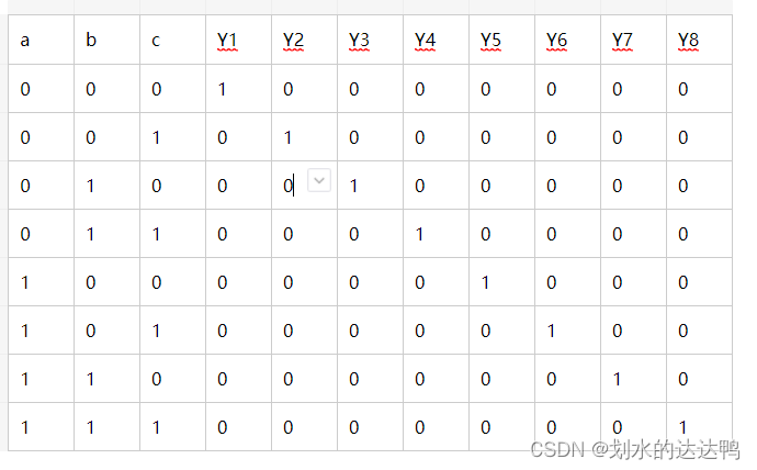
其真值表为:
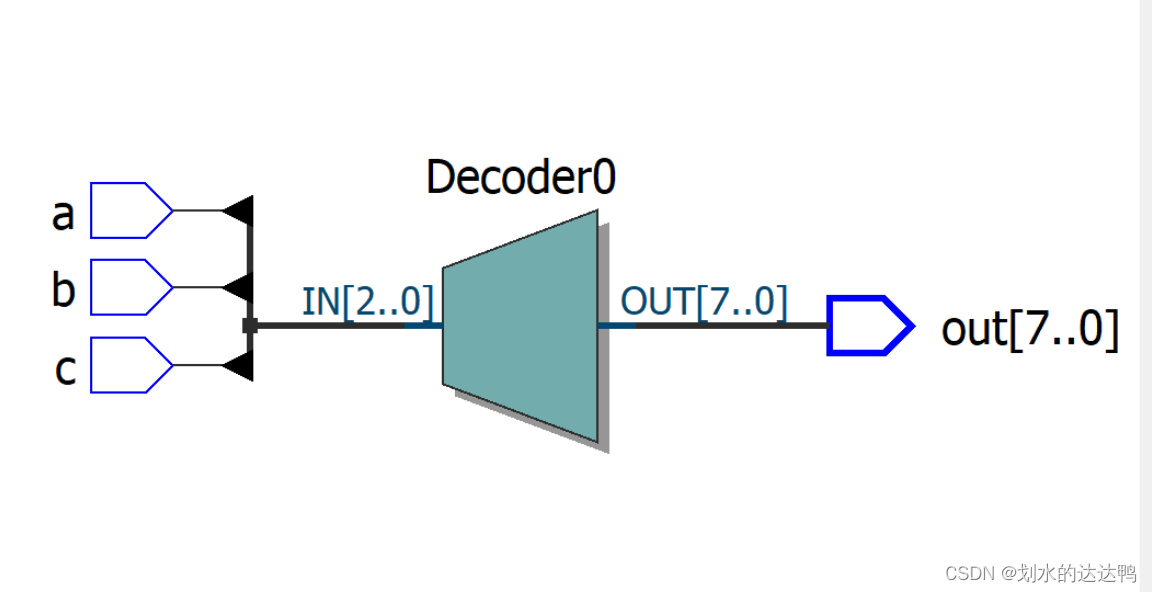
2、用Verilog编程设计一个3-8译码器,生成RTL原理电路图
代码为:
module D3_8(
	a,
	b,
	c,
	out
);
input a; //输入端口a
input b; //输入端口b
input c; //输入端口c
output [7:0]out;//输出端口out

reg [7:0]out;
always@(a,b,c)
begin
	case({a,b,c})
	3'b000:out = 8'b0000_0001;
	3'b001:out = 8'b0000_0010;
	3'b010:out = 8'b0000_0100;
	3'b011:out = 8'b0000_1000;
	3'b100:out = 8'b0001_0000;
	3'b101:out = 8'b0010_0000;
	3'b110:out = 8'b0100_0000;
	3'b111:out = 8'b1000_0000;
	endcase
end
endmodule
RTL电路为:
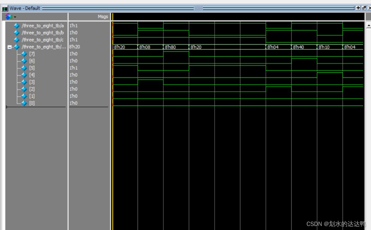
3、编写一个仿真测试文件,对3-8译码器进行仿真测试,输出测试波形图和Transcript结果
modelsim电路仿真文件为:
timescale 1ns/1ns

 module three_to_eight_tb();
 reg  a;
 reg  b;
 reg  c;
 wire   [7:0]   out;
 initial    begin
    a <= 1'b1;
    b <= 1'b0;
    c <= 1'b1;
 end
 //a:产生随机数,模拟 a 的输入情况
 always #10 a <= {$random} % 2;
 //b:产生随机数,模拟 b 的输入情况
 always #10 b <= {$random} % 2;
 //c:产生随机数,模拟c 的输入情况
 always #10 c <= {$random} % 2;
 initial begin
    $timeformat(-9, 0, "ns", 6);
    $monitor("@time %t:a=%b b=%b c=%b out=%b",$time,a,b,c,out);
 end
 three_to_eight three_to_eight_ins
 (
    .a(a),
    .b(b),
    .c(c),
    .out(out)
 );
 endmodule
仿真结果:
4、回答问题
(1)Verilog 综合生成的3-8译码器电路原理图与原始设计电路存在什么差异? 仿真测试生成的结果是否与真值表一致?
答:使用不同的技术库或综合设置可能会导致综合工具做出不同的选择,从而产生差异。在Verilog设计中,仿真测试应该与真值表一致。然而,综合后的电路可能在实际硬件中运行,因此仿真测试结果与真值表的一致性并不总是绝对的。
(2) Verilog代码设计的3-8译码器模块的输出信号为何要定义为 reg类型而不用默认wire(导线)类型?改成wire型是否可以? (即是否可以把 output reg [7:0] out 改为 output [7:0] out) 修改后会出现什么错误?为什么会出错?
答:在Verilog中,reg 和 wire 分别用于表示寄存器类型和导线类型。默认情况下,output 端口的信号类型是 wire,因此你可以直接写 output [7:0] out,而不必显式指定为 reg。修改为 output [7:0] out 不会导致错误,因为输出端口的默认类型是 wire。这是因为在组合逻辑中,信号之间的连接通常使用 wire 类型。然而,在某些情况下,你可能需要使用 reg 类型的输出信号,比如在时序逻辑中,如在 always 块中存储信号的状态。
如果确实需要在 output 中使用 reg 类型,可以显式声明为 output reg [7:0] out。这通常在时序逻辑中需要存储输出状态时使用。如果在组合逻辑中使用 reg 类型,可能会导致一些综合工具给出的警告,因为在组合逻辑中,通常使用 wire 类型更为合适。
总的来说,对于组合逻辑,可以使用默认的 wire 类型,而对于时序逻辑,可能需要使用 reg 类型。如果在组合逻辑中使用了 reg 类型,Verilog 编译器通常会发出警告,但不会导致编译错误。
二
1、用Verilog的门级描述方式写一个“1位全加器”, 生成RTL电路,与Logsim的“1位全加器”进行对比。
其verilog代码为:
module FullAdder_gate_level (
  input A, B, Cin,
  output Sum, Cout
);
  wire X1, X2, X3, X4;
  assign X1 = A ^ B;
  assign X2 = X1 ^ Cin;
  assign X3 = A & B;
  assign X4 = X1 & Cin;
  assign Sum = X2;
  assign Cout = X3 | X4;

endmodule
RTL电路图为:
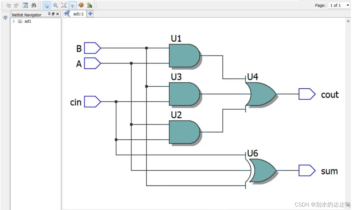
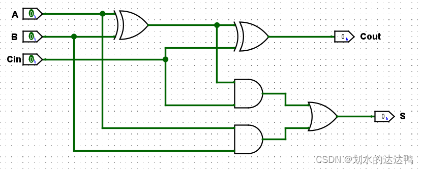
logisim电路图为:
2、用Verilog模块调用子模块的方式,用4个上面的“1位全加器”级联方式,构成一个“4位全加器”(即串行全加器),生成RTL电路,与Logsim的“4位全加器”电路进行对比
四位全加器verilog代码:
module FourBitAdder_gate_level (
  input [3:0] A, B, Cin,
  output [3:0] Sum, Cout
);
  wire C1, C2, C3;
  wire S1, S2, S3;
  FullAdder_gate_level f1 (.A(A[0]), .B(B[0]), .Cin(Cin), .Sum(S1), .Cout(C1));
  FullAdder_gate_level f2 (.A(A[1]), .B(B[1]), .Cin(C1), .Sum(S2), .Cout(C2));
  FullAdder_gate_level f3 (.A(A[2]), .B(B[2]), .Cin(C2), .Sum(S3), .Cout(C3));
  FullAdder_gate_level f4 (.A(A[3]), .B(B[3]), .Cin(C3), .Sum(Sum[3]), .Cout(Cout));
endmodule
module FullAdder_gate_level (
  input A, B, Cin,
  output Sum, Cout
);
  wire X1, X2, X3, X4;
  assign X1 = A ^ B;
  assign X2 = X1 ^ Cin;
  assign X3 = A & B;
  assign X4 = X1 & Cin;
  assign Sum = X2;
  assign Cout = X3 | X4;
endmodule
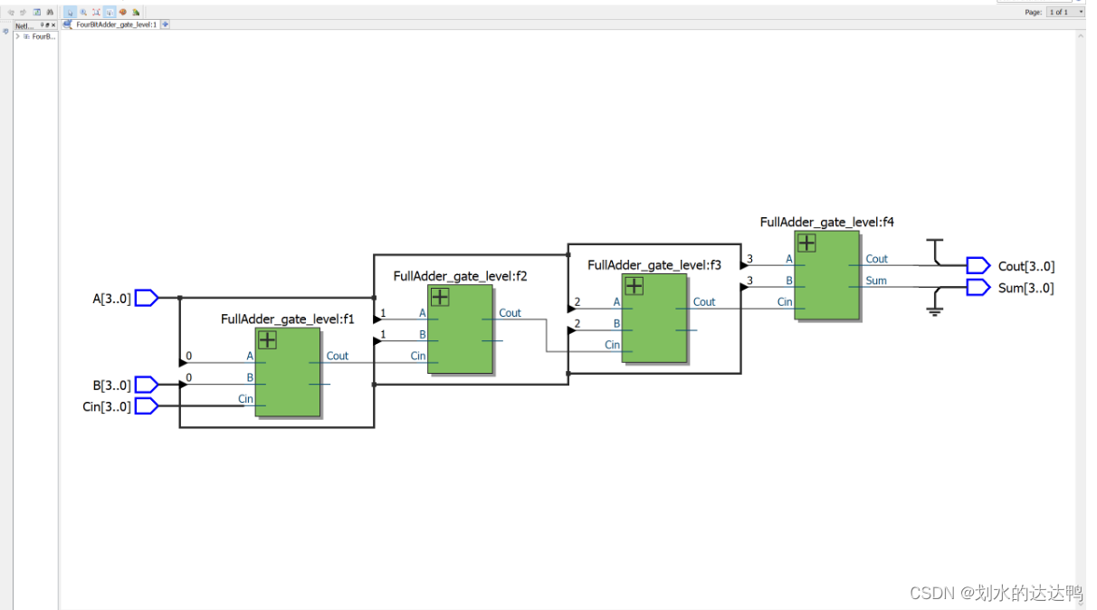
RTL电路图为:
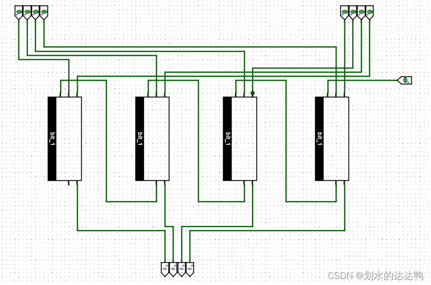
logisim电路图为:
3、采用Verilog的行为级方式重新完成上面的1和2
1位全加器verilog代码:
module FullAdder_functional_level (
  input A, B, Cin,
  output Sum, Cout
);
  assign {Cout, Sum} = A + B + Cin;
endmodule
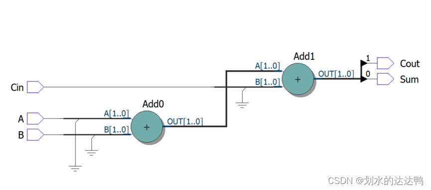
1位全加器RTL电路图:
四位全加器verilog代码:
module FullAdder_functional_level (
  input A, B, Cin,
  output Sum, Cout
);
  assign {Cout, Sum} = A + B + Cin;
endmodule
module FourBitAdder_functional_level (
  input [3:0] A, B, Cin,
  output [3:0] Sum,
  output Cout
);
  wire c1, c2, c3;
  FullAdder_functional_level fa1(A[0], B[0], Cin, Sum[0], c1);
  FullAdder_functional_level fa2(A[1], B[1], c1, Sum[1], c2);
  FullAdder_functional_level fa3(A[2], B[2], c2, Sum[2], c3);
  FullAdder_functional_level fa4(A[3], B[3], c3, Sum[3], Cout);
endmodule
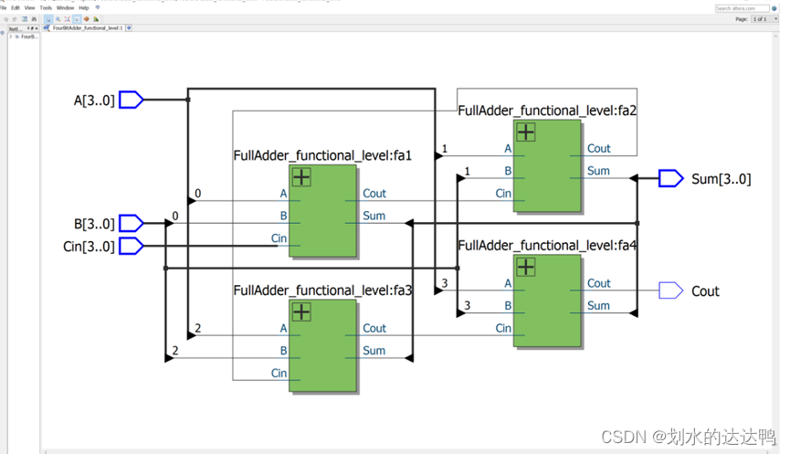
4位全加器RTL电路图:
4、采用Verilog设计一个8位全加器模块
8位全加器verilog代码:
module eight_bit_adder(
    input [7:0] a,
    input [7:0] b,
    input cin,
    output [7:0] sum,
    output cout
);
wire [7:0] c;
full_adder fa0(a[0], b[0], cin, sum[0], c[0]);
full_adder fa1(a[1], b[1], c[0], sum[1], c[1]);
full_adder fa2(a[2], b[2], c[1], sum[2], c[2]);
full_adder fa3(a[3], b[3], c[2], sum[3], c[3]);
full_adder fa4(a[4], b[4], c[3], sum[4], c[4]);
full_adder fa5(a[5], b[5], c[4], sum[5], c[5]);
full_adder fa6(a[6], b[6], c[5], sum[6], c[6]);
full_adder fa7(a[7], b[7], c[6], sum[7], cout);
endmodule
module full_adder(
    input a,
    input b,
    input cin,
    output sum,
    output cout
);
assign sum = a ^ b ^ cin;
assign cout = (a & b) | (a & cin) | (b & cin);
endmodule
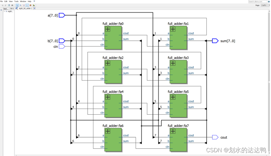
8位全加器RTL电路图:


 8639
8639


 被折叠的 条评论
为什么被折叠?
被折叠的 条评论
为什么被折叠?
 到【灌水乐园】发言


