


the important one for hardware is AMBA AXI, which is
Arm Microcontroller Bus Architecture Advanced eXtensible Interface
see Arm's own documentation for a controlled learning experience:
for a comprehensive coverage of all generations of AXI protocols, see/download:
http://www.gstitt.ece.ufl.edu/courses/fall15/eel4720_5721/labs/refs/AXI4_specification.pdf
Ready/Valid Protocol
Drake Enterprises – Ready/Valid Protocol Primer
Introduction
In digital logic design, the ready/valid protocol is a simple and common handshake process for one component to transmit data to another component in the same clock domain. Every FIFO implements a version of this protocol on its ports, whether the signals are called "ready/valid", or "full/push" and "pop/empty". Also, ready/valid signals are used as the flow control mechanism for every channel of the popular AMBA AXI high performance on-chip interconnect.
Despite its ubiquitous application, there is no de-facto standard implementation. Engineers routinely implement ad-hoc ready/valid logic in every codebase they work with. In this primer, we will describe the protocol in detail, propose standard naming conventions, and write some reusable SystemVerilog interface code to bolster design verification.
The code we will write is not advanced, but familiarity with SystemVerilog Assertions (SVA) will be helpful.
Protocol Description
Assume we have two components in a hardware design with a unidirectional data flow. A "Transmitter" (Tx) sends data to a "Receiver" (Rx). The Transmitter and Receiver are equal partners in this data exchange. That is, the Transmitter cannot force the Receiver to consume data, and the Receiver cannot force the Transmitter to produce data. For a transfer of data to happen, the two sides need to "shake hands". The Transmitter needs to have "valid" data, and the Receiver needs to be "ready" to receive the data.
Figure 1 shows a block diagram of the basic ready/valid/data components. Note that the "ready" and "valid" signals are single wires, but the "data" signal is a bus composed of multiple wires transmitting in parallel.
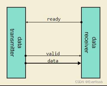
Figure 1: Data Transmitter and Receiver
Aside Regarding Component Names
Phil Karlton once said "there are only two hard things in Computer Science: cache invalidation and naming things." The book Microarchitecture of Network-on-Chip Routers uses the terms "sender" and receiver". The AMBA Specification uses the terms "source" and "destination", or "master" and "slave". I have seen other documents use terms such as "producer" and "consumer", and so on.
I have arbitrarily chosen the names "Transmitter" and "Receiver" because
- they are unambiguous - one transmits data, the other receives it
- they are commonly used in digital signal processing (DSP)
- they both have the same number of syllables
- I like the "Tx" and "Rx" abbreviations
Link State
Since there are two control bits, the link can be in four possible states. We will name those states according to the following table.
| State Name | ready | valid | Description |
|---|---|---|---|
| Idle | 0 | 0 | Transmitter does not have valid data. |
| Wait for Ready | 0 | 1 | Transmitter has valid data, but Receiver is not ready for it. Data will NOT be transferred. |
| Wait for Valid | 1 | 0 | Receiver is ready for data, but transmitter has none. |
| Transfer | 1 | 1 | Transmitter has valid data, and Receiver is ready for it. Data will be transferred. |
According to the AMBA Specification, section A.3.2.1, there are two rules governing ready/valid behavior:
- A transmitter is not permitted to wait until
READY is asserted before asserting VALID[VALID asserted before READY].
==> the above line, with the crossed out section, is actually from the Arm doc, but it is missing vital context, without which, it can only logically be the corrected version.
see the doc for yourself: Documentation – Arm Developer
In Figure 3.2, the source presents the address, data or control information after T1 and asserts the VALID signal. The destination asserts the READY signal after T2, and the source must keep its information stable until the transfer occurs at T3, when this assertion is recognized.
Figure 3.2. VALID before READY handshake
A source is not permitted to wait until READY is asserted before asserting VALID.
==> here clearly when READY is asserted before VALID, the source is certainly 1 entire transaction ahead of receiver, hence, allowed to wait
====> which in general is really the intuitive case of VALID being asserted before READY.
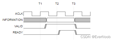
- Once VALID is asserted it must remain asserted until the handshake occurs, at a rising clock edge at which VALID and READY are both asserted.
The first rule is a performance requirement. To achieve full bandwidth on the link, the ready and valid signals must be independent.
The second rule places a restriction on exiting the Wait for Ready state. Once the transmitter has valid data, it is illegal to renege on the transfer. It must wait until the receiver is ready for it.
AMBA does not restrict whether the ready signal is allowed to assert and later deassert without a handshake. However, some implementations may desire this extra level of strictness. For example, a FIFO is "ready" when it has a slot available. If it ever deasserted its ready signal without a data push, that would be a serious error that we need to uncover. I will refer to this extra strict version of the protocol as the "stable ready" requirement.
Figure 2 shows the legal state transitions.
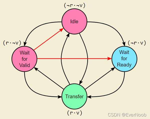
Figure 2: Ready/Valid Link State
For the less strict version of the protocol with no stable ready requirement, we can effectively merge the Idle and Wait for Valid states, marked in red.
For the more strict version of the protocol with stable ready requirement, we can remove the arrows marked in red. Both of the Wait for ... states may only transition to Transfer state.
We will formalize these rules a little later with SystemVerilog assertions.
Link Signal Timing
Figure 3 shows a timing diagram of three data words being transferred. The style of the waveform mimics debuggers such as Verdi and Simvision. Signals are driven immediately after the clock edge with no visible delay. The upward arrows on the clock signal indicate clock edges when data transfer events occur.
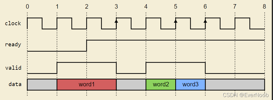
Figure 3: Ready/Valid Protocol Waveform Debugger View
For convenience, the follow table summarizes the events:
| Time | Receiver Ready? | Transmitter Valid? | State |
|---|---|---|---|
| 1 | No | No | Idle |
| 2 | No | Yes | WaitForReady |
| 3 | Yes | Yes | Transfer Word #1 |
| 4 | Yes | No | WaitForValid |
| 5 | Yes | Yes | Transfer Word #2 |
| 6 | Yes | Yes | Transfer Word #3 |
| 7 | Yes | No | WaitForValid |
Aside Regarding Waveform Perspective
When analyzing logical protocols that are implemented using real-world, analog technologies such as wires and transistors, we need to draw the waveform diagram with appropriate propagation delays. Unfortunately, there is no standard frame of reference for the link.
Figure 4 shows a more realistic representation of Figure 3, but from the perspective of the Transmitter. Notice that the ready signal arrives late.
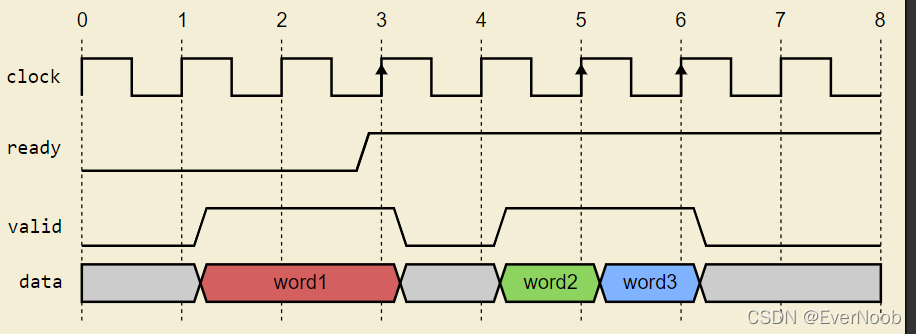
Figure 4: Ready/Valid Protocol Transmit Perspective View
Figure 5 shows a similarly realistic representation of Figure 3, but this time from the perspective of the Receiver. Notice that the valid/data signals arrive late.
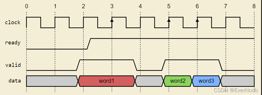
Figure 5: Ready/Valid Protocol Receive Perspective View
These diagrams help visualize important implementation details. For example, the designer of the Transmitter should avoid adding significant logic to the ready input, because it might violate the setup time.
In addition, considering the handshake signal propagation delays can clarify their meaning. When the Receiver drives ready=1 onto the wire, it does not yet know whether the Transmitter will send data. In plain English, it sends the message: "if you transmit data on this cycle, I am ready for it". Similary, when the Transmitter drives valid=1 onto the wire, it sends the message: "if you are ready, I will transmit this data to you". Both the ready and valid signals contain propositional logic that can only be satisfied after the signal propagation delay.
Interface Implementation Conventions
When using ready/valid interfaces in SystemVerilog code, bundle the signals together and use a consistent naming convention. Different projects have different rules, but I recommend at least the following:
- Order the ready/valid/data signals consistently
- Use a common interface name prefix
- Use standard ready/valid/data name suffixes
For example, here is a good module parameter/port list for a generic FIFO.
module Fifo #(
    parameter type T = logic [7:0]
) (
    // Read Port
    input  logic read_ready,
    output logic read_valid,
    output T     read_data,

    // Write Port
    output logic write_ready,
    input  logic write_valid,
    input  T     write_data,

    input logic clock,
    input logic reset
);
    ...
endmodule : Fifo
A module may have several ready/valid interfaces for several purposes. In order to find them quickly using a command line grep or debugger glob pattern match, all members of an interface bundle should have a common prefix. This particular FIFO has a read and write port, which are given 'read_', and 'write_' prefixes, respectively.
Use the standard suffix names '_ready', '_valid', and '_data'. Do not use clever abbreviations like '_rdy', and '_vld'. Do not sacrifice clarity for brevity. The AMBA specification does not abbreviate these signals names; neither should we.
Also, do not use port direction naming conventions such as '_o' for "output" and '_i' for "input". It should be obvious to the reader which signals are inputs and outputs. For example, a FIFO's write port should have 'valid' and 'data' inputs.
Do not use a SystemVerilog interface to implement the ports. SV interfaces provide ergonomic benefit for passing around large bundles of signals, but they will end up costing more in tool support and maintenance issues than they ever pay in benenfits for a collection of only three signals. Reserve usage of interfaces for verification components such as UVM agents.
Formal Checks
SystemVerilog assertions are one of the most productive ways of finding and fixing logical errors and coverage holes. In this section, we will write a standard suite of ready/valid protocol assertions that can be copied and pasted for every interface instance.
Before delving into the implementation details, to reduce the amount of boilerplate required to write concurrent assumptions, assertions, and cover properties, we will first define three text replacement preprocessor macros. For background on this best practice, read section 8 of SystemVerilog Assertions Bindfiles & Best Known Practices for Simple SVA Usage, presented at Synopsys User Group (SNUG) 2016.
`define ASSUME(name, expr, clock, reset) \
name: assume property ( \
    @(posedge clock) disable iff (reset) (expr) \
);

`define ASSERT(name, expr, clock, reset) \
name: assert property ( \
    @(posedge clock) disable iff (reset) (expr) \
);

`define COVER(name, expr, clock, reset) \
name: cover property ( \
    @(posedge clock) disable iff (reset) (expr) \
);
Different tools treat assumptions, assertions, and cover properties differently. For example, for simulators there is no difference between an assumption and an assertion -- they are both just dynamic checks. Formal verification (FV) tools, on the other hand, create logic proofs using assertions, and use assumptions to constrain the stimulus for those proofs. See IEEE 1800-2017 for a more detailed description. For our purposes, we will use assumptions for module inputs, and assertions for module outputs.
Note that applying checks to both inputs and outputs will cause a small but measurable simulation performance degradation due to duplicated work. The inputs of one module are the outputs of another, so we end up doing each check twice. The benefits of debuggability outweigh the costs of simulation time, but if we desire maximum efficiency, we can fix this overlap by disabling all assumptions in simulation.
Always Check for Xes on Control Signals
Interface control signals should never be unknown (i.e. "X", not in {0,1}{0,1}). Also, whenever valid=1 is asserted, its corresponding data should never have have unknown bits. Never underestimate the amount of problems your team will discover by writing X checks to catch uninitialized state.
Using the FIFO module ports from above, with "write" and "read" ready/valid interfaces, the code for this is straightforward:
/*** Transmit (Tx) ***/
// Ready must never be unknown
`ASSUME(RV_Tx_NeverReadyUnknown,
    !$isunknown(read_ready),
    clock, reset)

// Valid/Data must never be unknown
`ASSERT(RV_Tx_NeverValidUnknown,
    !$isunknown(read_valid),
    clock, reset)
`ASSERT(RV_Tx_NeverDataUnknown,
    read_valid |-> !$isunknown(read_data),
    clock, reset)

/*** Receive (Rx) ***/
// Ready must never be unknown
`ASSERT(RV_Rx_NeverReadyUnknown,
    !$isunknown(write_ready),
    clock, reset)

// Valid/Data must never be unknown
`ASSUME(RV_Rx_NeverValidUnknown,
    !$isunknown(write_valid),
    clock, reset)
`ASSUME(RV_Rx_NeverDataUnknown,
    write_valid |-> !$isunknown(write_data),
    clock, reset)
Note that the SystemVerilog $isunknown system task will return 1 if any bits of the input are unknown.
Protocol Violations
Using Figure 2 as a reference, the Transmitter or Receiver commit a protocol violation whenever they cause an invalid state transition on the link. When the link is in "Wait for Ready" state, the Transmitter may not deassert valid on the next cycle. For the strict protocol with stable ready requirement, when the link is in "Wait for Valid" state, the Receiver may not deassert ready on the next cycle. Finally, the Transmitter may not put new data onto the link until after the current data has been successfully transferred.
For the less strict protocol with no stable ready requirement, do NOT use the assumptions/assertions with *_ReadyStable suffix.
/*** Transmit (Tx) ***/
// Ready must remain stable until Valid/Data
// Note: Optional
`ASSUME(RV_Tx_ReadyStable,
    (read_ready && !read_valid) |=> read_ready,
    clock, reset)

// Valid/Data must remain stable until Ready
`ASSERT(RV_Tx_ValidDataStable,
    (!read_ready && read_valid) |=> (read_valid && $stable(read_data)),
    clock, reset)

/*** Receive (Rx) ***/
// Ready must remain stable until Valid/Data
// Note: Optional
`ASSERT(RV_Rx_ReadyStable,
    (write_ready && !write_valid) |=> write_ready,
    clock, reset)

// Valid/Data must remain stable until Ready
`ASSUME(RV_Rx_ValidDataStable,
    (!write_ready && write_valid) |=> (write_valid && $stable(write_data)),
    clock, reset)
A full explanation of SystemVerilog Assertions (SVA) is beyond the scope of this primer, but let's take a closer look at the RV_Tx_ValidDataStable code. The statement X |=> Y means: "If X is true on this clock cycle, then check that Y is true on the next clock cycle". The $stable(X) statement means: "The value of X on this clock cycle is the same as it was on the previous clock cycle." Putting it all together, in plain English the assertions means: "If the link is in Wait for Ready state on this clock cycle, then both valid/data must stay the same on the next clock cycle".
Cover Properties
After we spend the time to write a thorough test suite, coverage collection will help verify that the tests are exercising all the desired functionality.
First, we want to cover data transfers. If no data transfers have occurred on the interface, we have not actually tested anything.
The following code increments a coverage counter whenever the links are in the "Transfer" state.
// Cover data transfer
`COVER(RV_Tx_Transfer, read_ready && read_valid, clock, reset)
`COVER(RV_Rx_Transfer, write_ready && write_valid, clock, reset)
Another important cover property is "backpressure". When downstream components are blocking new data from being received, they are said to "backpressure" the upstream components. Without going into a full discussion of queueing fundamentals, it is important to exercise backpressure on all components in order to verify that storage buffers are adequately sized.
The following code increments a coverage counter whenever the links are in the "Wait for Valid" (backpressure) state:
// Cover backpressure
`COVER(RV_Tx_Backpressure, !read_ready && read_valid, clock, reset)
`COVER(RV_Rx_Backpressure, !write_ready && write_valid, clock, reset)
Checker Component Methodology
In the previous sections, we have defined several assumptions, assertions, and coverpoints. Good coding practice suggests we group these related items together in a container.
SystemVerilog provides a design element called a "checker" for this purpose, but I do not recommend using it. Not only are checkers not parameterizable, but they are not supported by EDA tools nearly as well as modules. Keep it simple, and just use a module for a reusable checker container.
In addition to a type parameter for the data inputs, we should have parameters for the following:
- Selectively enable transmitter and receiver checks.
- Selectively enable the strict ready stable requirement.
For example:
module CheckReadyValid #(
    parameter type T = logic [7:0]
    parameter bit Tx = 1'b0,
    parameter bit TxReadyStable = 1'b0,
    parameter bit Rx = 1'b0,
    parameter bit RxReadyStable = 1'b0
) (
    input logic ready,
    input logic valid,
    input T     data,

    input logic clock,
    input logic reset
);

// Check either Tx or Rx interface, not both (or neither)
if (Tx == Rx) begin
    $fatal(1, "Expected Tx != Rx, got Tx=%0d Rx=%0d", Tx, Rx);
end

if (Tx) begin : gen_tx_checks
    `ASSUME(NeverReadyUnknown, !$isunknown(read_ready), clock, reset)
    `ASSERT(NeverValidUnknown, !$isunknown(read_valid), clock, reset)
    `ASSERT(NeverDataUnknown,
        read_valid |-> !$isunknown(read_data),
        clock, reset)
    if (TxReadyStable) begin : gen_ready_stable
        `ASSUME(ReadyStable,
            (read_ready && !read_valid) |=> read_ready,
            clock, reset)
    end : gen_ready_stable
    `ASSERT(ValidDataStable,
        (!read_ready && read_valid) |=> (read_valid && $stable(read_data)),
        clock, reset)
    `COVER(Transfer, read_ready && read_valid, clock, reset)
    `COVER(Backpressure, !read_ready && read_valid, clock, reset)
end : gen_tx_checks

if (Rx) begin : gen_rx_checks
    `ASSERT(NeverReadyUnknown, !$isunknown(write_ready), clock, reset)
    `ASSUME(NeverValidUnknown, !$isunknown(write_valid), clock, reset)
    `ASSUME(NeverDataUnknown,
        write_valid |-> !$isunknown(write_data),
        clock, reset)
    if (RxReadyStable) begin : gen_ready_stable
        `ASSERT(ReadyStable,
            (write_ready && !write_valid) |=> write_ready,
            clock, reset)
    end : gen_ready_stable
    `ASSUME(ValidDataStable,
        (!write_ready && write_valid) |=> (write_valid && $stable(write_data)),
        clock, reset)
    `COVER(Transfer, write_ready && write_valid, clock, reset)
    `COVER(Backpressure, !write_ready && write_valid, clock, reset)
end : gen_rx_checks

endmodule : CheckReadyValid
Conclusion
The ready/valid protocol is a fundamental tool in the logic designer's toolbox. A modern CPU or GPU performs billions of ready/valid data transfers per second. This simple, two-wire handshake is at the heart of computer science and engineering. We must carefully study, master, and standardize every aspect of it.
Whether you are integrating an IP core into a bleeding edge SoC with a sophisticated AMBA on-chip interconnect, or just making the LEDs blink on your weekend FPGA side project, I sincerely hope this ready/valid primer using SystemVerilog will come in handy.
AXI protocol overview
AXI is an interface specification that defines the interface of IP blocks, rather than the interconnect itself.
The following diagram shows how AXI is used to interface an interconnect component:
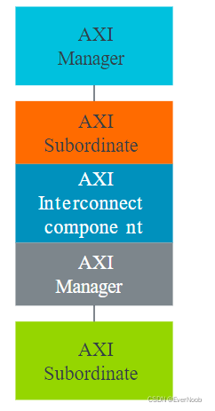
There are only two AXI interface types, manager and subordinate. These interface types are symmetrical. All AXI connections are between manager interfaces and subordinate interfaces.
AXI interconnect interfaces contain the same signals, which makes integration of different IP relatively simple. The previous diagram shows how AXI connections join manager and subordinate interfaces. The direct connection gives maximum bandwidth between the manager and subordinate components with no extra logic. And with AXI, there is only a single protocol to validate.
AXI in a multi-manager system
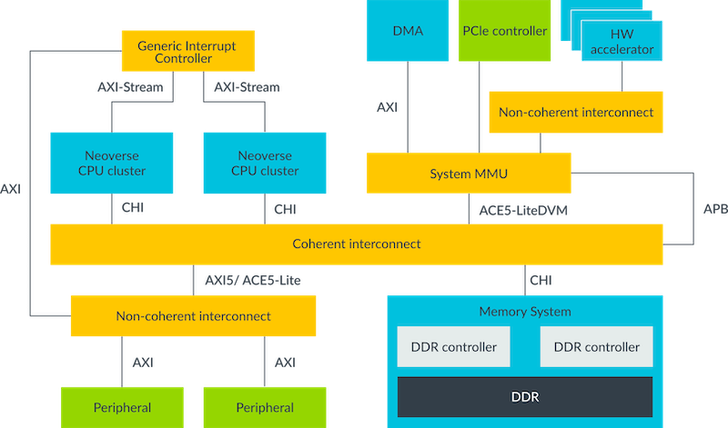
The following diagram shows a simplified example of an SoC system, which is composed of managers, subordinates, and the interconnect that links them all:
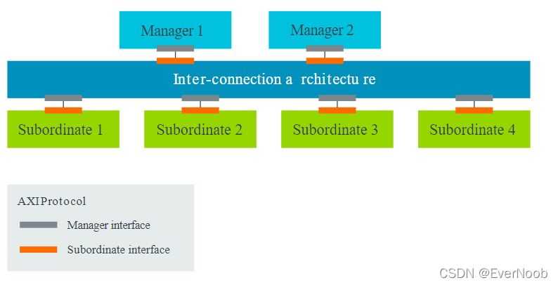
An Arm processor is an example of a manager, and a simple example of a subordinate is a memory controller.
The AXI protocol defines the signals and timing of the point-to-point connections between manager and subordinates.
Note: The AXI protocol is a point-to-point specification, not a bus specification. Therefore, it describes only the signals and timing between interfaces.
The previous diagram shows that each AXI manager interface is connected to a single AXI subordinate interface. Where multiple managers and subordinates are involved, an interconnect fabric is required. This interconnect fabric also implements subordinate and manager interfaces, where the AXI protocol is implemented.
The following diagram shows that the interconnect is a complex element that requires its own AXI manager and subordinate interfaces to communicate with external function blocks:
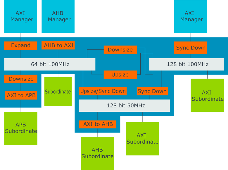
The following diagram shows an example of an SoC with various processors and function blocks:

The previous diagram shows all the connections where AXI is used. You can see that AXI3 and AXI4 are used within the same SoC, which is common practice. In such cases, the interconnect performs the protocol conversion between the different AXI interfaces.
AXI channels
The AXI specification describes a point-to-point protocol between two interfaces: a manager and a subordinate. The following diagram shows the five main channels that each AXI interface uses for communication:
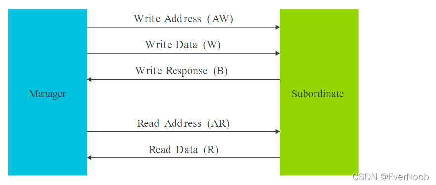
Write operations use the following channels:
- The manager sends an address on the Write Address (AW) channel and transfers data on the Write Data (W) channel to the subordinate.
- The subordinate writes the received data to the specified address. Once the subordinate has completed the write operation, it responds with a message to the manager on the Write Response (B) channel.
Read operations use the following channels:
- The manager sends the address it wants to read on the Read Address (AR) channel.
-
The subordinate sends the data from the requested address to the manager on the Read Data (R) channel.
The subordinate can also return an error message on the Read Data (R) channel. An error occurs if, for example, the address is not valid, or the data is corrupted, or the access does not have the right security permission.
Note: Each channel is unidirectional, so a separate Write Response channel is needed to pass responses back to the manager. However, there is no need for a Read Response channel, because a read response is passed as part of the Read Data channel.
Using separate address and data channels for read and write transfers helps to maximize the bandwidth of the interface. There is no timing relationship between the groups of read and write channels. This means that a read sequence can happen at the same time as a write sequence.
Each of these five channels contains several signals, and all these signals in each channel have the prefix as follows:
- AW for signals on the Write Address channel
- AR for signals on the Read Address channel
- W for signals on the Write Data channel
- R for signals on the Read Data channel
- B for signals on the Write Response channel
Note: B stands for buffered, because the response from the subordinate happens after all writes have completed.
Main AXI features
The AXI protocol has several key features that are designed to improve bandwidth and latency of data transfers and transactions, as you can see here:
Independent read and write channels
AXI supports two different sets of channels, one for write operations, and one for read operations. Having two independent sets of channel helps to improve the bandwidth performances of the interfaces. This is because read and write operations can happen at the same time.
Multiple outstanding addresses
AXI allows for multiple outstanding addresses. This means that a manager can issue transactions without waiting for earlier transactions to complete. This can improve system performance because it enables parallel processing of transactions.
No strict timing relationship between address and data operations
With AXI, there is no strict timing relationship between the address and data operations. This means that, for example, a manager could issue a write address on the Write Address channel, but there is no time requirement for when the manager has to provide the corresponding data to write on the Write Data channel.
Support for unaligned data transfers
For any burst that is made up of data transfers wider than one byte, the first bytes accessed can be unaligned with the natural address boundary. For example, a 32-bit data packet that starts at a byte address of 0x1002 is not aligned to the natural 32-bit address boundary.
Out-of-order transaction completion
Out-of-order transaction completion is possible with AXI. The AXI protocol includes transaction identifiers, and there is no restriction on the completion of transactions with different ID values. This means that a single physical port can support out-of-order transactions by acting as several logical ports, each of which handles its transactions in order.
Burst transactions based on start address
AXI managers only issue the starting address for the first transfer. For any following transfers, the subordinate will calculate the next transfer address based on the burst type.
What is AMBA, and why use it?
The Advanced Microcontroller Bus Architecture, or AMBA, is an open-standard, on-chip interconnect specification for the connection and management of functional blocks in system-on-a-chip (SoC) designs.
Essentially, AMBA protocols define how functional blocks communicate with each other.
The following diagram shows an example of an SoC design. This SoC has several functional blocks that use AMBA protocols, like AXI, to communicate with each other:
Where is AMBA used?
AMBA simplifies the development of designs with multiple processors and large numbers of controllers and peripherals. However, the scope of AMBA has increased over time, going far beyond just microcontroller devices.
Today, AMBA is widely used in a range of ASIC and SoC parts. These parts include applications processors that are used in devices like IoT subsystems, smartphones, and networking SoCs.
Why use AMBA?
AMBA provides several benefits:
Efficient IP reuse
IP reuse is an essential component in reducing SoC development costs and timescales. AMBA specifications provide the interface standard that enables IP reuse. Therefore, thousands of SoCs, and IP products, are using AMBA interfaces.
Flexibility
AMBA offers the flexibility to work with a range of SoCs. IP reuse requires a common standard while supporting a wide variety of SoCs with different power, performance, and area requirements. Arm offers a range of interface specifications that are optimized for these different requirements.
Compatibility
A standard interface specification, like AMBA, allows compatibility between IP components from different design teams or vendors.
Support
AMBA is well supported. It is widely implemented and supported throughout the semiconductor industry, including support from third-party IP products and tools.
Bus interface standards like AMBA, are differentiated through the performance that they enable. The two main characteristics of bus interface performance are:
Bandwidth
The rate at which data can be driven across the interface. In a synchronous system, the maximum bandwidth is limited by the product of the clock speed and the width of the data bus.
Latency
The delay between the initiation and completion of a transaction. In a burst-based system, the latency figure often refers to the completion of the first transfer rather than the entire burst.
The efficiency of your interface depends on the extent to which it achieves the maximum bandwidth with zero latency.
How has AMBA evolved?
AMBA has evolved over the years to meet the demands of processors and new technologies, as shown in the following diagram:
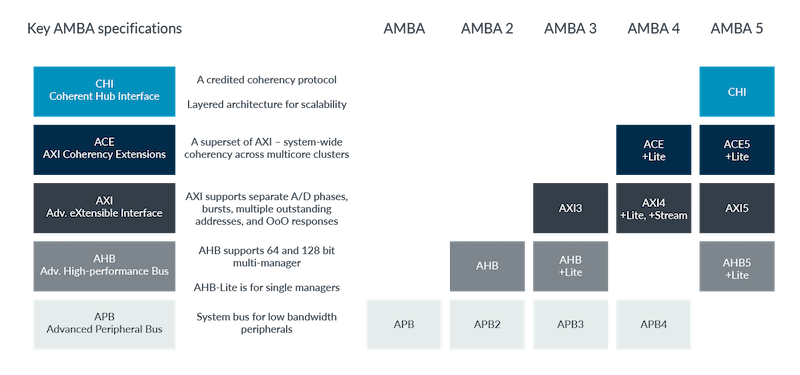
AMBA
Arm introduced AMBA in the late 1990s. The first AMBA buses were the Advanced System Bus (ASB) and the Advanced Peripheral Bus (APB). ASB has been superseded by more recent protocols, while APB is still widely used today.
APB is designed for low-bandwidth control accesses, for example, register interfaces on system peripherals. This bus has a simple address and data phase and a low complexity signal list.
AMBA 2
In 1999, AMBA 2 added the AMBA High-performance Bus (AHB), which is a single clock-edge protocol. A simple transaction on the AHB consists of an address phase and a subsequent data phase. Access to the target device is controlled through a MUX, admitting access to one manager at a time. AHB is pipelined for performance, while APB is not pipelined for design simplicity.
AMBA 3
In 2003, Arm introduced the third generation, AMBA 3, which includes ATB and AHB-Lite.
Advanced Trace Bus (ATB), is part of the CoreSight on-chip debug and trace solution.
AHB-Lite is a subset of AHB. This subset simplifies the design for a bus with a single manager.
Advanced eXtensible Interface (AXI), the third generation of AMBA interface defined in the AMBA 3 specification, is targeted at high performance, high clock frequency system designs. AXI includes features that make it suitable for high-speed submicrometer interconnect.
AMBA 4
In 2010, the AMBA 4 specifications were introduced, starting with AMBA 4 AXI4 and then AMBA 4 AXI Coherency Extensions (ACE) in 2011.
ACE extends AXI with additional signaling introducing system-wide coherency. This system-wide coherency allows multiple processors to share memory and enables technology like big.LITTLE processing. At the same time, the ACE-Lite protocol enables one-way coherency. One-way coherency enables a network interface to read from the caches of a fully coherent ACE processor.
The AXI4-Stream protocol is designed for unidirectional data transfers from manager to subordinate with reduced signal routing, which is ideal for implementation in FPGAs.
AMBA 5
In 2014, the AMBA 5 Coherent Hub Interface (CHI) specification was introduced, with a redesigned high-speed transport layer and features designed to reduce congestion. There have been several editions of the CHI protocol, and each new version adds new features.
In 2016, the AHB-Lite protocol was updated to AHB5, to complement the Armv8-M architecture, and extend the TrustZone security foundation from the processor to the system.
In 2019, the AMBA Adaptive Traffic Profiles (ATP) was introduced. ATP complements the existing AMBA protocols and is used for modeling high-level memory access behavior in a concise, simple, and portable way.
AXI5, ACE5 and ACE5-Lite extend prior generations, to include a number of performance and scalability features to align with and complement AMBA CHI. Some of the new features and options include:
- Support for high frequency, non-blocking coherent data transfer between many processors.
- A layered model to allow separation of communication and transport protocols for flexible topologies, such as a cross-bar, ring, mesh or ad hoc.
- Cache stashing to allow accelerators or IO devices to stash critical data within a CPU cache for low latency access.
- Far atomic operations enable the interconnect to perform high-frequency updates to shared data.
- End-to-end data protection and poisoning signalling.


 被折叠的 条评论
为什么被折叠?
被折叠的 条评论
为什么被折叠?
 到【灌水乐园】发言


