


 这篇博客详细介绍了C2000系列微控制器中ADC模块的功能,包括28379D的ADC特性,如16位和12位模式,以及EOC中断、SOC排序器、信号模式(单端和差分)等。内容涵盖了ADC的中断配置、采样窗口、触发信号分析,并提供了PPB的偏移校准、限值检测和中断信号解析。
1. 28379D-ADC模块
绪论:
关于ADC模块,原先只总结了28335的,而且内容零散,不太满意,所以打算将28379D模块的ADC系统地总结一下,不得不说这个系列功能太强大了,EOC,PPB…
ADC-器件概述:
模拟子系统
– 多达四个模数转换器 (ADC)
– 16 位模式
– 每个转换器的吞吐量为 1.1MSPS(系统吞
吐量高达 4.4MSPS)
– 差分输入
– 多达 12 个外部通道
– 12 位模式
– 每个转换器的吞吐量为 3.5MSPS(系统吞
吐量高达 14MSPS)
– 单端输入
– 多达 24 个外部通道
– 每个 ADC 上有单个采样与保持 (S/H) 电路
– ADC 转换的硬件集成后置处理
– 饱和偏移校准
– 定点计算误差
– 具有中断功能的高、 低和过零比较
– 触发至采样延迟捕捉
– 八个具有 12 位数模转换器 (DAC) 参考的窗口化
比较器
– 3 个 12 位缓冲 DAC 输出
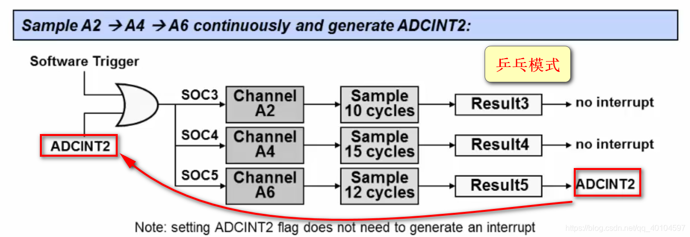
1. ADC-EOC
简述:
Each SOC has a corresponding(相应的) end-of-conversion (EOC) signal. This EOC signal can be used to trigger
an ADC interrupt. The ADC can be configured to generate the EOC pulse at either the end of the acquisition window or at the end of the voltage conversion. This is configured using the bit INTPULSEPOS
in the ADCCTL1 register. See Section 11.14, for exact EOC pulse location.
个人翻译:每一个SOC子模块会有一个相应的EOC信号。这个EOC信号可以被用于触发ADC中断。ADC可以配置在【采样窗口末尾】或者【电压转化末尾】产生EOC脉冲信号。此配置用ADCCTL1 寄存器中的INTPULSEPOS位来设置。
人话:每一个SOC事件转换完成之后可以产生一个EOC信号,那么这个EOC信号又可以作为一个SOC触发事件,是不是有点像在打乒乓球。
2. ADC-SOC 排序器
SOC-Trigger Operation(SOC的触发源)
简述:
Each SOC can be configured to start on one of many input triggers. The primary trigger select for SOCx is
in the ADCSOCxCTL.TRIGSEL register, which can select between:
• Disabled (software only) 不使能(仅软件强制模式适用)
• CPU Timers 0/1/2 (from each C28x core present)
• GPIO: Input X-Bar INPUT5
• ADCSOCA or ADCSOCB from each ePWM module
参考:

2. ADC-Signal Mode 信号模式
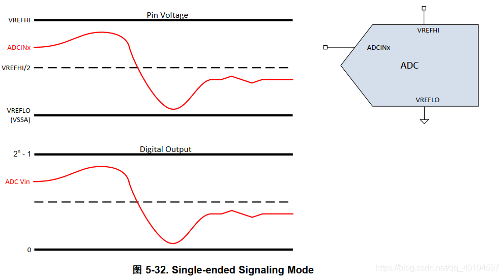
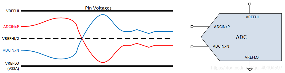
简述(来自datasheet):
The ADC supports two signal modes: single-ended and differential. In single-ended mode, the input
voltage to the converter is sampled through a single pin (ADCINx), referenced to VREFLO. In differential
signaling mode, the input voltage to the converter is sampled through a pair of input pins, one of which is
the positive input (ADCINxP) and the other is the negative input (ADCINxN). The actual input voltage is
the difference between the two (ADCINxP – ADCINxN). 图 5-31 shows the differential signaling mode. 图
5-32 shows the single-ended signaling mode.
翻译一下上述内容
ADC模块支持两种信号模式:
- single-ended(单端的)
- differential(差分)。
single-ended单端模式:
在single-ended模式中输入电压是通过一个信号引脚(ADCINx)信号采样到达转换器的。参考电压是VREFLO。
differential差分模式:
在differential模式中,这个输入电压是通过一对输入引脚采样到达转换器的,一个引脚是正极输入 (ADCINxP)另一个是负极输入 (ADCINxN)。事实上,在 (ADCINxP)和 (ADCINxN)引脚的输入电压是不同的。
[截图不是完整的]!
疑难杂症
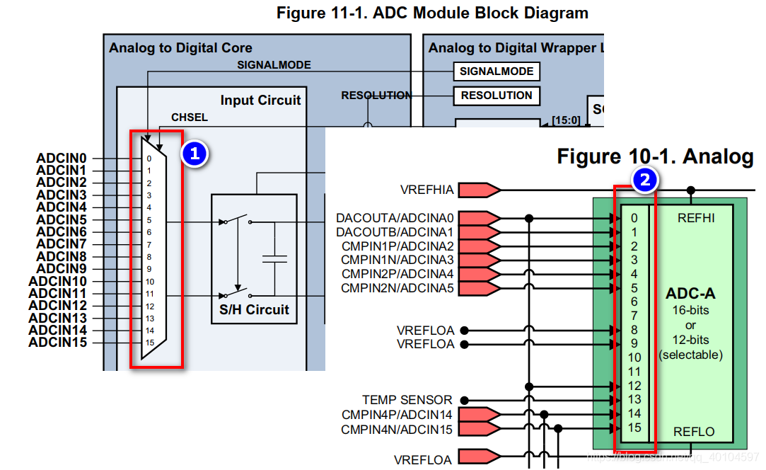
如下图所示:AdcaRegs.ADCSOC0CTL.bit.CHSEL此项设置的具体含义不是很理解…
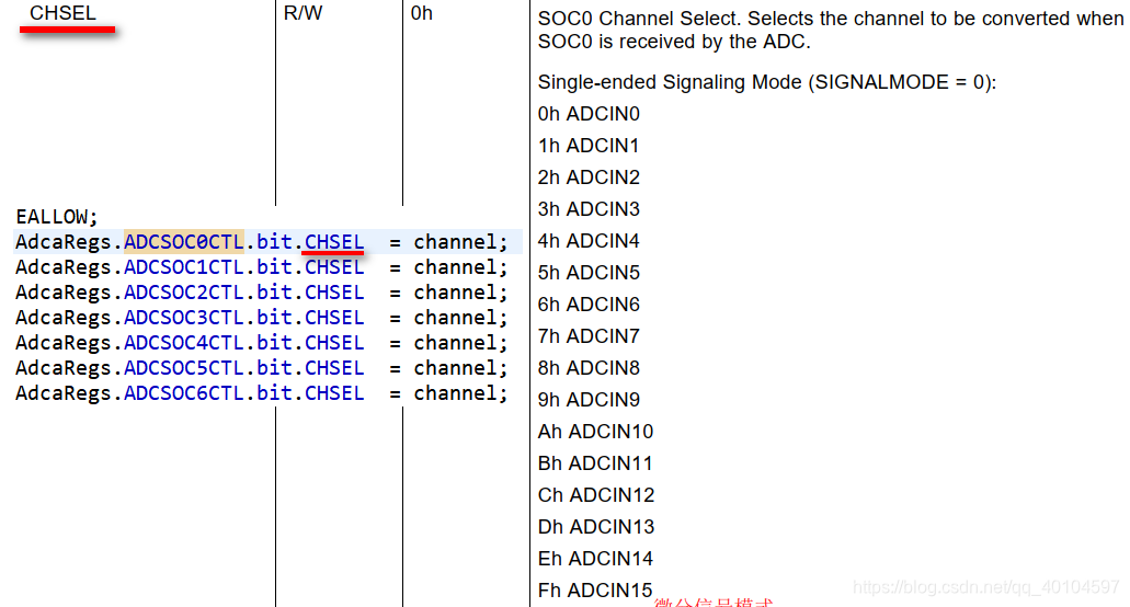
ADC采样窗:
待完善
网上的一些总结:
- 任意一次SOC事件都可以触发中断【认为可信】
- SOCx触发==》采样保持==》最终结果是在存到ADCRESULTx?【半信半疑】
如:SOC0 ===》ADCRESULT0?
ADC程序配置示例:
主要想记录一下自己宝贵的注释 ^ _ ^
void ConfigureADC(void)
{

    EALLOW;

    //
    //write configurations
    //
    AdcaRegs.ADCCTL2.bit.PRESCALE = 6; //set ADCCLK divider to /4
    /*
     * 参数1:选择哪一组ADC(A/B/C/D)
     * 参数2:选择ADC精度(12bit/16bit)
     * 参数3:选择ADC模式(SINGLE/DIFFERENTIAL)
     * */
    AdcSetMode(ADC_ADCA, ADC_RESOLUTION_12BIT, ADC_SIGNALMODE_SINGLE);//

    //
    //Set pulse positions to late   设置脉冲位置延迟
    //
    AdcaRegs.ADCCTL1.bit.INTPULSEPOS = 1;

    /* ADC上电 */
    //
    //power up the ADC
    //
    AdcaRegs.ADCCTL1.bit.ADCPWDNZ = 1;

    //
    //delay for 1ms to allow ADC time to power up
    //
    DELAY_US(1000);

    EDIS;
}

//
// SetupADCContinuous - Setup the ADC to continuously convert on one channel  设置ADC在一个通道上连续转换
//
void SetupADCContinuous(Uint16 channel)
{

    Uint16 acqps;

    //
    // Determine minimum acquisition window (in SYSCLKS) based on resolution
    //
    if(ADC_RESOLUTION_12BIT == AdcaRegs.ADCCTL2
最低0.47元/天 解锁文章


 1325
1325

 被折叠的 条评论
为什么被折叠?
被折叠的 条评论
为什么被折叠?
 到【灌水乐园】发言


