


1.参考代码示例
PRJ_M66_4.3.3\boards\apollo4l_blue_eb\examples\peripherals\adc_measure\src\adc_measure.c
本篇基于Apollo4BlueLite 4.3.3版本的SDK中adc_measure.c示例的代码进行分析。
2. 代码流程
(1)初始化一路GPIO作为ADC输入
(2)初始化ADC模块,同时配置使能中断
(3)启动ADC软件触发模式
(4)这样ADC就会根据配置的采样频率循环采样
(5)该示例中会在中断处理函数中打印采样结果
3. 代码分析
(1)设置ADC输入pin脚
通过该函数实现把指定GPIO引脚设置为ADC输入的功能。在Apollo4BlueLite芯片中定义了8路GPIO可以被配置为ADC输入pin脚,分别为GPIO12~GPIO19
// Set a pin to act as our ADC input

am_hal_gpio_pinconfig(ADC_INPUT_PIN, g_ADC_PIN_CFG);
(2)ADC初始化函数
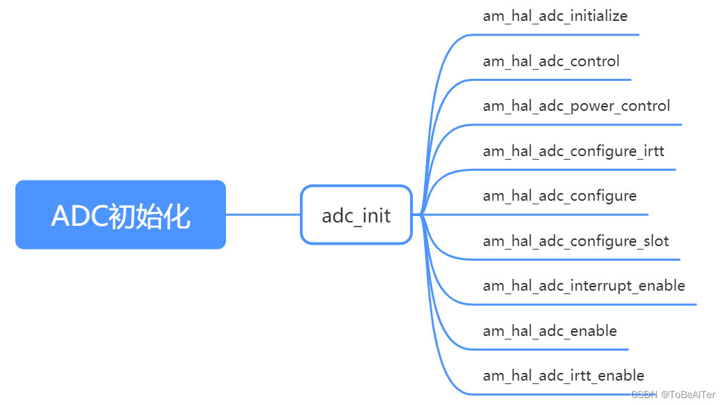
- uint32_t am_hal_adc_initialize(uint32_t ui32Module, void **ppHandle)
该函数实现通过设备编号初始化ADC设备(ADC Device Handle)
- uint32_t am_hal_adc_control(void *pHandle, am_hal_adc_request_e eRequest, void *pArgs)
该函数为ADC特有的控制功能函数,初始化流程中eRequest为AM_HAL_ADC_REQ_CORRECTION_TRIMS_GET,这里是用来获取当前ADC设备的校准偏移和增益
- uint32_t am_hal_adc_power_control(void *pHandle, am_hal_sysctrl_power_state_e ePowerState, bool bRetainState)
该函数用来给ADC模块启动供电,ePowerState为AM_HAL_SYSCTRL_WAKE
- uint32_t am_hal_adc_configure_irtt(void *pHandle, am_hal_adc_irtt_config_t *pConfig)
该函数用来配置ADC内部重复触发采样的定时器
- uint32_t am_hal_adc_configure(void *pHandle, am_hal_adc_config_t *psConfig)
该函数用来配置ADC模块,包括设置ADC时钟源始终频率,时钟极性(上升沿采样或下降沿采样),触发源选择,采样间隔是否下电,采样模式(单次采样/连续采样)等
- uint32_t am_hal_adc_configure_slot(void *pHandle, uint32_t ui32SlotNumber, am_hal_adc_slot_config_t *pSlotConfig)
该函数用来配置ADC模块的slot,包括配置采样值的平均数量,绑定输入通道,转换精度等
- uint32_t am_hal_adc_interrupt_enable(void *pHandle, uint32_t ui32IntMask)
该函数用来使能ADC的中断
- uint32_t am_hal_adc_enable(void *pHandle)
该函数用来使能ADC模块
- uint32_t am_hal_adc_irtt_enable(void *pHandle)
该函数用来使能内部重复触发定时器
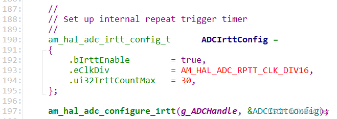
4. ADC寄存器
4.1 ADC IRTT寄存器
(1)ADC模块通过IRTT (Internal Repeating Trigger Timer)来配置采样频率,首先我们需要了解一下IRTT寄存器,如下图所示。
| Bits | Name | RW | Description | 备注 |
| 31 | TIMEREN | RW | ADC-internal trigger timer enable. DIS = 0x0 - Disable the ADC-internal trigger timer. EN = 0x1 - Enable the ADC-internal trigger timer. | 内部触发定时器使用寄存器 |
| 30:19 | RSVD | RO | RESERVED. | |
| 18:16 | CLKDIV | RW | Configure number of divide-by-2 of clock source as input to trigger counter. (Max value of 5.) A value of 0 in this register would not divide down the ADC input clock. A value of 1 would divide the ADC input clock frequency by 2. A value of 5 would divide the ADC input clock frequency by 2^5 = 32. To update this value, first disable the INTTRIGTIMER by setting TIMEREN to DIS, change CLKDIV, and then reenable it INTTRIGTIMER by setting TIMEREN to EN again. | 采样时钟分频系数,在示例中ADC的输入时钟为HFRC_24MHz,CLKDIV=16,那么实际的采样频率为24MHz/16=1.5MHz |
| 15:10 | RSVD | RO | RESERVED. | |
| 9:0 | TIMERMAX | RW | Trigger counter count max, used as initial condition to trigger. Also used repeatedly each time counter reaches it to restart trigger timer at zero. To update this value, first disable the INTTRIGTIMER by setting TIMEREN to DIS, change TIMERMAX, and then reenable it INTTRIGTIMER by setting TIMEREN to EN again. | 该参数定义了每隔多少个时钟周期,ADC会采样一次并得到一个采样结果 |
(2)结合示例代码理解
如下图代码所示,采样频率为1.5MHz,IrttCountMax=30,实际上采样间隔为1s/1.5MHZ*30≈20us
这里需要注意目前代码中支持的分频系数为1,2,4,6,IrttCountMax的取值范围为1~1023(因为寄存器为10bit,最大值为0x3FF)
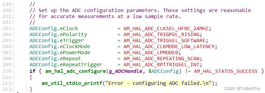
4.2 ADC配置寄存器
(1)ADC模块有专门的配置寄存器进行基本状态的配置,下图为CFG寄存器信息
| Bits | Name | RW | Description | 备注 |
| 31:26 | RSVD | RO | RESERVED. | |
| 25:24 | CLKSEL | RW | Select the source and frequency for the general purpose ADC clock. HFRC_24MHZ is the only valid GP ADC clock selection and must be configured for proper operation. HFRC_48MHZ = 0x0 - This setting must not be used for CLKSEL for the GP ADC even though it is the default setting. Software must set CLKSEL to HFRC_24MHZ after any reset event and before enabling the ADC. HFRC_48MHZ1 = 0x1 - This setting must not be used for CLKSEL for the GP ADC. HFRC_24MHZ = 0x2 - HFRC clock at 24 MHz. This setting is the only valid setting for the GP ADC. HFRC2_48MHZ = 0x3 - This setting must not be used for CLKSEL for the GP ADC. | GP ADC目前只能设置时钟源为24MHz |
| 23:21 | RSVD | RO | RESERVED. | |
| 20 | RPTTRIGSEL | RW | This bit selects which periodic trigger to use with RPTEN = 1. TMR = 0x0 - Trigger from on-chip timer. INT = 0x1 - Trigger from ADC-internal timer. | 选择ADC采样定时器,INT模式对应timer_7 |
| 19 | TRIGPOL | RW | This bit selects the ADC trigger polarity for external off chip triggers. RISING_EDGE = 0x0 - Trigger on rising edge. FALLING_EDGE = 0x1 - Trigger on falling edge. | 配置采样上升沿触发或者下降沿触发 |
| 18:16 | TRIGSEL | RW | Select the ADC trigger source. EXT0 = 0x0 - Off chip External Trigger0 (ADC_ET0) EXT1 = 0x1 - Off chip External Trigger1 (ADC_ET1) EXT2 = 0x2 - Off chip External Trigger2 (ADC_ET2) EXT3 = 0x3 - Off chip External Trigger3 (ADC_ET3) VCOMP = 0x4 - Voltage Comparator Output SWT = 0x7 - Software Trigger | 选择ADC的触发源,这里我们一般情况选用的是SWT软件触发 |
| 15:13 | RSVD | RO | RESERVED. | |
| 12 | DFIFORDEN | RW | Destructive FIFO Read Enable. Setting this will enable FIFO pop upon reading the FIFOPR register. DIS = 0x0 - Destructive Reads are prevented. Reads to the FIFOPR register will not POP an entry off the FIFO. EN = 0x1 - Reads to the FIFOPR registger will automatically pop an entry off the FIFO. | Destructive FIFO Read Enable:这个设置可以实现在读取FIFOPR寄存器时弹出FIFO中的数据。一般情况都会使能。 |
| 11:5 | RSVD | RO | RESERVED. | |
| 4 | CKMODE | RW | Clock mode register LPCKMODE = 0x0 - Disable the clock between scans for LPMODE0. Set LPCKMODE to 0x1 while configuring the ADC. LLCKMODE = 0x1 - Low Latency Clock Mode. When set, HFRC and the adc_clk will remain on while in functioning in LPMODE0. | LPMODE=0,CKMODE=1,在ADC采样过程中始终保持HFRC和ADC clock使能 |
| 3 | LPMODE | RW | Select power mode to enter between active scans. MODE0 = 0x0 - Low Power Mode 0. Leaves the ADC fully powered between scans with minimum latency between a trigger event and sample data collection. MODE1 = 0x1 - Low Power Mode 1. Powers down all circuity and clocks associated with the ADC until the next trigger event. Between scans, the reference buffer requires up to 50us of delay from a scan trigger event before the conversion will commence while operating in this mode. | |
| 2 | RPTEN | RW | This bit enables Repeating Scan Mode. SINGLE_SCAN = 0x0 - In Single Scan Mode, the ADC will complete a single scan upon each trigger event. REPEATING_SCAN = 0x1 - In Repeating Scan Mode, the ADC will complete its first scan upon the initial trigger event and all subsequent scans will occur at regular intervals defined by the configuration programmed for the CTTMRA3 timer or the ADC-internal timer (see the RPTTRIGSEL field) until the timer is disabled or the ADC is disabled. When disabling the ADC (setting ADCEN to '0'), the RPTEN bit should be cleared. | 设置单次采样或者连续采样 |
| 1 | RSVD | RO | RESERVED. | |
| 0 | ADCEN | RW | This bit enables the ADC module. While the ADC is enabled, the ADCCFG and SLOT Configuration regsiter settings must remain stable and unchanged. All configuration register settings, slot configuration settings and window comparison settings should be written prior to setting the ADCEN bit to '1'. DIS = 0x0 - Disable the ADC module. EN = 0x1 - Enable the ADC module. | 使能ADC模块 |
(2)结合示例代码理解
在示例中配置Clock为24MHz,上升沿触发,触发源为软件触发,LPMODE0模式(采样过程中保持HFRC和ADC clock),使能了重复采样模式,使用内部定时器触发
4.3 SLOT配置寄存器
(1)Apollo4BlueLite ADC模块有8个slot,可以和前端8路外部输入pin脚进行关联,每个slot都有独立的寄存器进行配置。
| Bits | Name | RW | Description | 备注 |
| 31:27 | RSVD | RO | RESERVED. | |
| 26:24 | ADSEL0 | RW | Select the number of measurements to average in the accumulate divide module for this slot. AVG_1_MSRMT = 0x0 - Average in 1 measurement in the accumulate divide module for this slot. AVG_2_MSRMTS = 0x1 - Average in 2 measurements in the accumulate divide module for this slot. AVG_4_MSRMTS = 0x2 - Average in 4 measurements in the accumulate divide module for this slot. AVG_8_MSRMT = 0x3 - Average in 8 measurements in the accumulate divide module for this slot. AVG_16_MSRMTS = 0x4 - Average in 16 measurements in the accumulate divide module for this slot. AVG_32_MSRMTS = 0x5 - Average in 32 measurements in the accumulate divide module for this slot. AVG_64_MSRMTS = 0x6 - Average in 64 measurements in the accumulate divide module for this slot. AVG_128_MSRMTS = 0x7 - Average in 128 measurements in the accumulate divide module for this slot. | 该寄存器配置手机指定的采样值后计算平均值作为一次采样结果保存在slot中 |
| 23:18 | TRKCYC0 | RW | Set additional input signal sampling/tracking time to the specified number of ADC clock cycles. (Note that a value of 0 in this register specifies the minimum required 5 cycles. A maximum of 64 specifies 69 cycles.) | 设置额外的输入信号采样/跟踪时间为指定的ADC时钟周期数。请注意,该寄存器中的值为0表示最小所需的5个周期。最大值为64,表示69个周期。目前代码中要求该值必须为32 |
| 17:16 | PRMODE0 | RW | Set the Precision Mode For Slot 0. P12B0 = 0x0 - 12-bit precision mode P12B1 = 0x1 - 12-bit precision mode P10B = 0x2 - 10-bit precision mode P8B = 0x3 - 8-bit precision mode | 设置ADC转换精度 |
| 15:12 | RSVD | RO | RESERVED. | |
| 11:8 | CHSEL0 | RW | Select one of the 14 channel inputs for this slot. SE0 = 0x0 - Single ended external GPIO connection to pad16. SE1 = 0x1 - Single ended external GPIO connection to pad29. SE2 = 0x2 - Single ended external GPIO connection to pad11. SE3 = 0x3 - Single ended external GPIO connection to pad31. SE4 = 0x4 - Single ended external GPIO connection to pad32. SE5 = 0x5 - Single ended external GPIO connection to pad33. SE6 = 0x6 - Single ended external GPIO connection to pad34. SE7 = 0x7 - Single ended external GPIO connection to pad35. TEMP = 0x8 - Internal temperature sensor. BATT = 0x9 - Internal voltage divide-by-3 connection. TESTMUX = 0xA - Analog testmux. VSS = 0xB - Input VSS. | 选择和当前slot绑定的输入通道,有14路通道可选 |
| 7:2 | RSVD | RO | RESERVED. | |
| 1 | WCEN0 | RW | This bit enables the window compare function for slot 0. WCEN = 0x1 - Enable the window compare for slot 0. WCDIS = 0x0 - Disable the window compare for slot 0. | 使用该bit使能窗口比较功能 |
| 0 | SLEN0 | RW | This bit enables slot 0 for ADC conversions. SLEN = 0x1 - Enable slot 0 for ADC conversions. SLDIS = 0x0 - Disable slot 0 for ADC conversions. | 使用该bit使能ADC转换 |
4.4 ADC FIFO寄存器
采样完成后采样结果会存储在FIFO中,Apollo4BlueLite ADC模块有16个FIFO,相关寄存器有FIFO和FIFOPR,其中FIFOPR是FIFO寄存器的Pop Read镜像副本,唯一的区别在于读取该寄存器将导致同时FIFO POP,这也可以通过向ADCFIFO寄存器写入来实现。注意:要启用破坏性读取,必须在CFG寄存器中设置DFIFORDEN位。。

| Bits | Name | RW | Description | 备注 |
| 31 | RSVD | RO | RESERVED. | |
| 30:28 | SLOTNUM | RO | Slot number associated with this FIFO data. | 通过该bit查询当前FIFO存储的数据关联的slot number |
| 27:20 | COUNT | RO | Number of valid entries in the ADC FIFO. | 表示FIFO中有效条目的总数,如果COUNT大于0,向该寄存器写入数据将会从FIFO中弹出一条FIFO条目,并将COUNT减1。 |
| 19:0 | DATA | RO | Oldest data in the FIFO. | 采样值 |
4.5 ADC中断寄存器
(1)中断相关寄存器有以下几种:
- INTEN(ADC Interrupts: Enable) 中断状态使能寄存器
- INTSAT(ADC Interrupts: Status) 中断状态寄存器
- INTCLR(ADC Interrupts: Clear) 中断状态清除寄存器
以上3个寄存器是完全对应的,在相同的bit实现中断的使能,状态查询和清除的功能,下面以使能寄存器为例进行讲解
| Bits | Name | RW | Description | 备注 |
| 31:12 | RSVD | RO | RESERVED. | |
| 11 | SATCB | RW | Saturation - Channel B (Slots 2 or 3) SATCBINT = 0x1 - Saturation, as specified by SAT configuration registers, occurred on either slot 2 or 3 (channel B) NONSATCBINT = 0x0 - No-Saturation | |
| 10 | SATCA | RW | Saturation - Channel A (Slots 0 or 1) SATCAINT = 0x1 - Saturation, as specified by SAT configuration registers, occurred on either slot 0 or 1 (channel A) NONSATCAINT = 0x0 - No Saturation | |
| 9 | ZXCB | RW | Zero Crossing - Channel B (Slots 2 or 3) ZXCBINT = 0x1 - Zero Crossing, as specified by ZX configuration registers, occurred on either slot 2 or 3 (channel B) NONZXCBINT = 0x0 - Non Zero Crossing | |
| 8 | ZXCA | RW | Zero Crossing - Channel A (Slots 0 or 1) ZXCAINT = 0x1 - Zero Crossing, as specified by ZX configuration registers, occurred on either slot 0 or 1 (channel A) NONZXCAINT = 0x0 - Non Zero Crossing | |
| 7 | DERR | RW | DMA Error Condition DMAERROR = 0x1 - DMA Error Condition Occurred NODMAERROR = 0x0 - DMA Error Condition did not Occurred | DMA错误中断 |
| 6 | DCMP | RW | DMA Transfer Complete DMACOMPLETE = 0x1 - DMA Completed a transfer DMAON = 0x0 - DMA completion is pending or not triggered. | DMA完成传输中断 |
| 5 | WCINC | RW | Window comparator voltage incursion interrupt. WCINCINT = 0x1 - Window comparator voltage incursion interrupt. WCINCNOINT = 0x0 - Not a Window comparator voltage incursion interrupt. | Voltage Incursion Interrupt 是在采样值低于窗口范围下限时触发 |
| 4 | WCEXC | RW | Window comparator voltage excursion interrupt. WCEXCINT = 0x1 - Window comparator voltage excursion interrupt. WCEXCNOINT = 0x0 - Not a Window comparator voltage excursion interrupt. | Voltage Excursion Interrupt 是在采样值超出窗口范围上限时触发 |
| 3 | FIFOOVR2 | RW | FIFO 100 percent full interrupt. FIFOFULLINT = 0x1 - FIFO 100 percent full interrupt. FIFOFULLNOINT = 0x0 - Not a FIFO 100 percent full interrupt. | FIFO中有效条目达到100%时上报中断,也就是FIFO COUNT为16时上报中断 |
| 2 | FIFOOVR1 | RW | FIFO 75 percent full interrupt. FIFO75INT = 0x1 - FIFO 75 percent full interrupt. FIFO75NOINT = 0x0 - Not FIFO 75 percent full interrupt. | FIFO中有效条目达到75%时上报中断,也就是FIFO COUNT为12时上报中断 |
| 1 | SCNCMP | RW | ADC scan complete interrupt. SCNCMPINT = 0x1 - ADC scan complete interrupt. SCNCMPNOINT = 0x0 - No ADC scan complete interrupt. | 扫描完成中断用于扫描模式下的多通道连续转换 |
| 0 | CNVCMP | RW | ADC conversion complete interrupt. CNVCMPINT = 0x1 - ADC conversion complete interrupt. CNVCMPNOINT = 0x0 - No ADC conversion complete interrupt. | 转换完成中断用于单次转换模式下的单通道转换 |
- INTSET(ADC Interrupts: Set) 中断状态设置寄存器,可以使ADC立即产生对应中断,一般调试使用


 895
895


 被折叠的 条评论
为什么被折叠?
被折叠的 条评论
为什么被折叠?
 到【灌水乐园】发言


