


 本文详细介绍了0.96寸OLED显示屏的构成,特别是SSD1306驱动芯片的工作原理,包括其接口、内存、供电、通信方式(如4线SPI和I2C)以及命令表。还涵盖了初始化过程和如何通过通信协议控制屏幕显示。
一、OLED模块简介
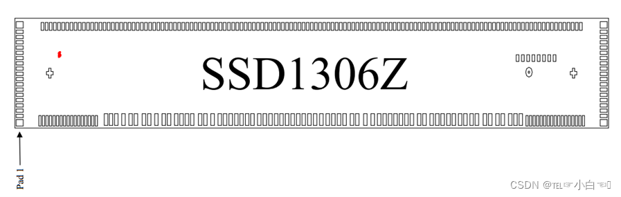
名称:0.96寸OLED显示屏
组成:一块PCB板(OLED的外围电路)、屏幕、驱动芯片(内嵌在屏幕下方)
驱动芯片:SSD1306(本篇是基于此芯片) / SSD1315(兼容)
像素:128*64像素
二、SSD1306驱动芯片
2.1 SSD1306简介
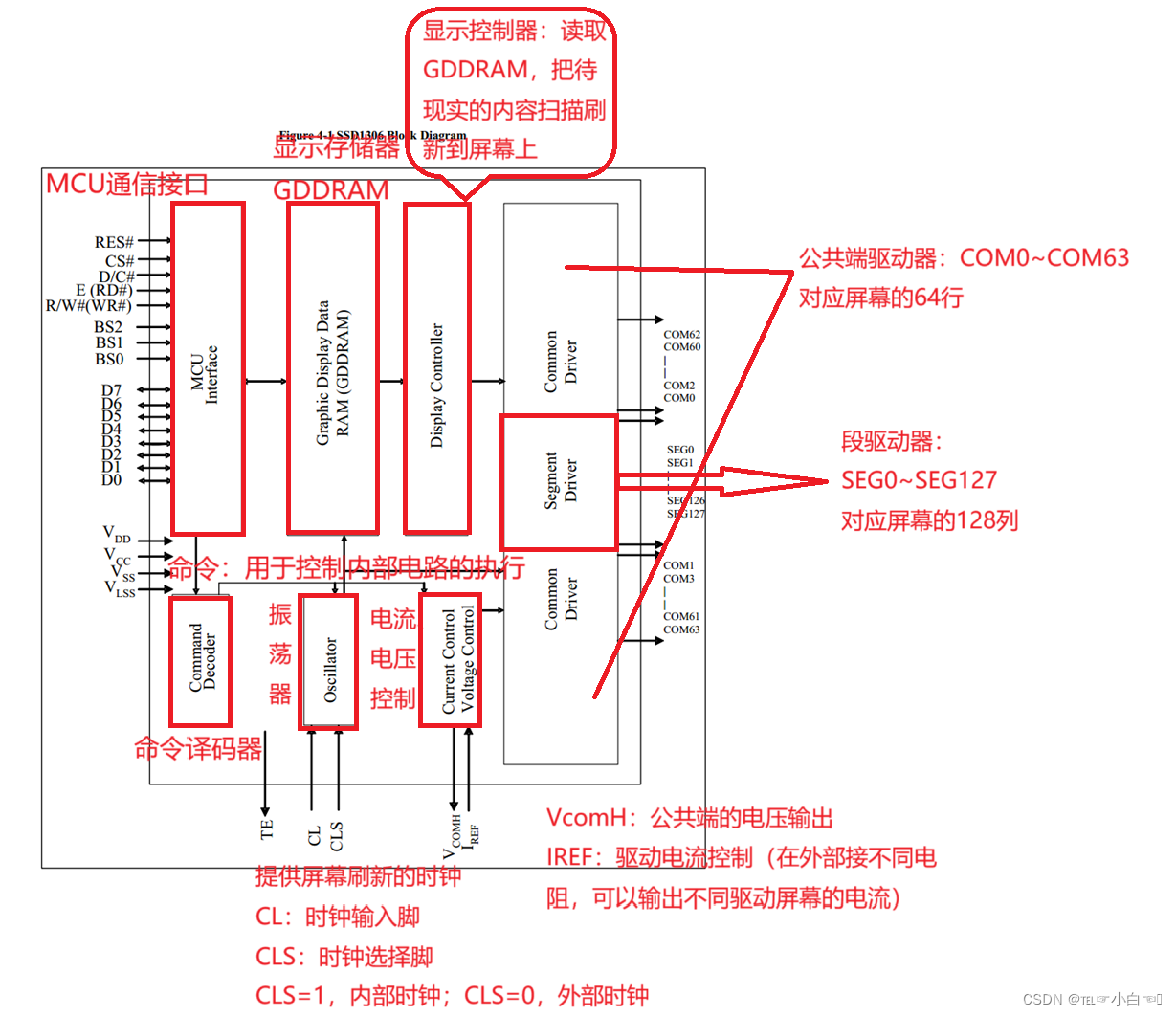
SSD1306是一款OLED/PLED点阵显示屏的控制器,可以嵌入在屏幕中,用于执行接收数据、显示存储、扫描刷新等任务
驱动接口:128个SEG引脚和64个COM引脚,对应128*64像素点阵显示屏
内置显示存储器(GDDRAM):128*64 bit (128*8 Byte)SRAM(1bit位对应一个像素点)
供电:VDD=1.65~3.3V(IC 逻辑,芯片内部的逻辑电路、存储器)、VCC=7~15V(面板驱动,点亮每个像素点)对于VCC而言,屏幕厂商已经在屏幕内部集成了一个升压电路,使用只需要开启即可
通信接口:8位6800/8080并行接口(SSD1315不支持)、3/4线SPI接口、I2C接口
通过通信引脚,把想要显示的内容数据发送给驱动芯片,当驱动芯片收到数据后,把数据存至SRAM显示存储器,通过时钟和扫描电路,将显示存储器的数据自动对应刷新到屏幕
因此,只需要通过通信协议,将待显示的内容数据存储至驱动芯片SRAM显示存储器中即可,屏幕显示由硬件自动完成
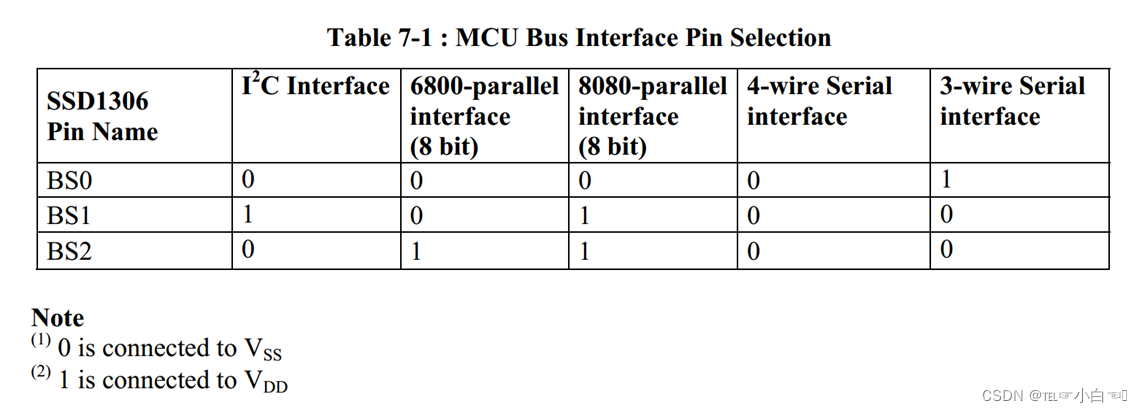
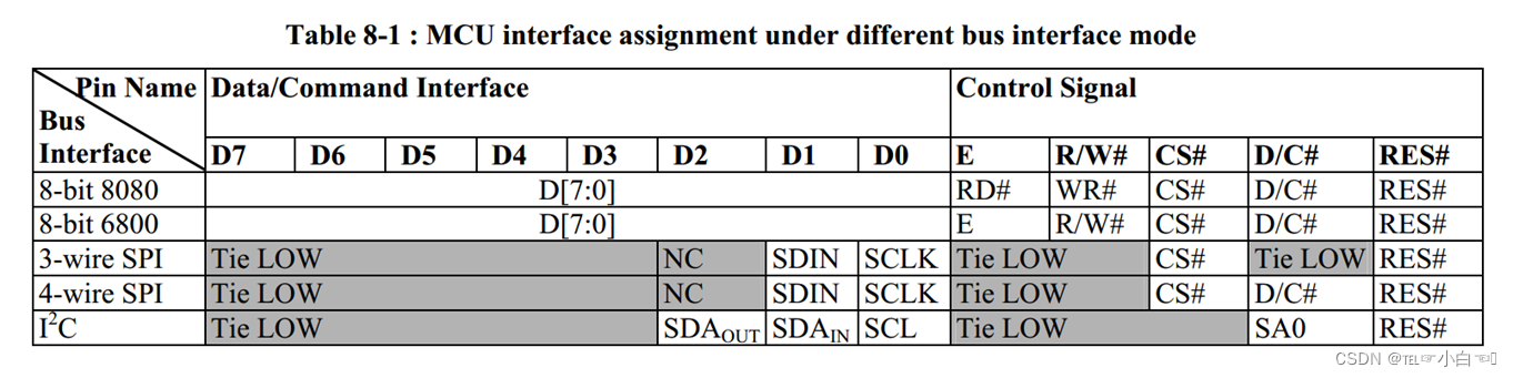
2.2 SSD1306框图及引脚定义
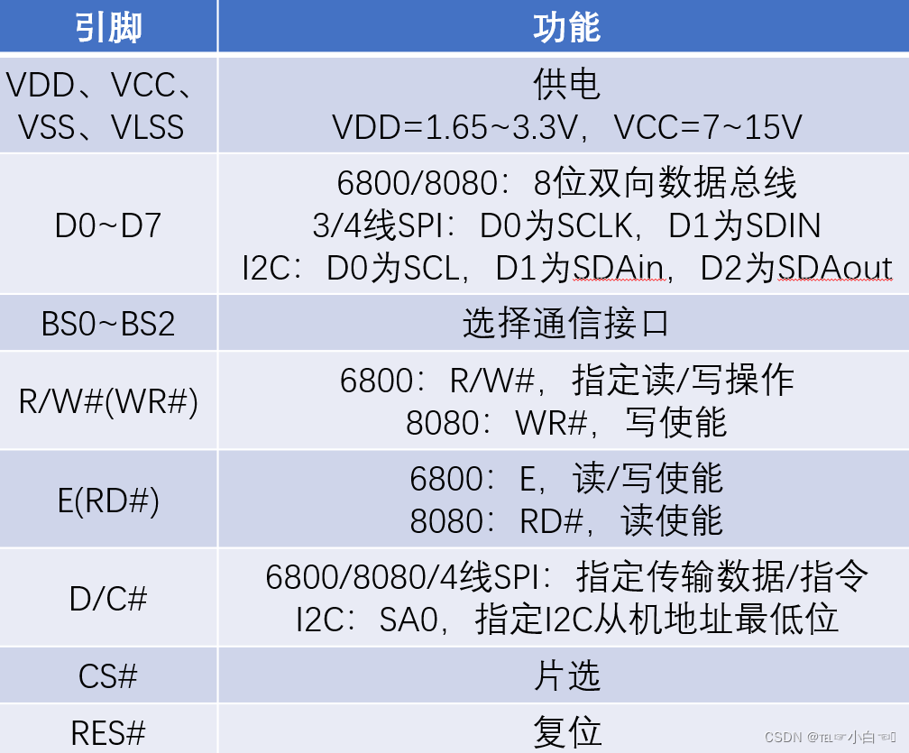
BS0~BS2选择通信接口:
其他引脚在不同通信协议下的意义:
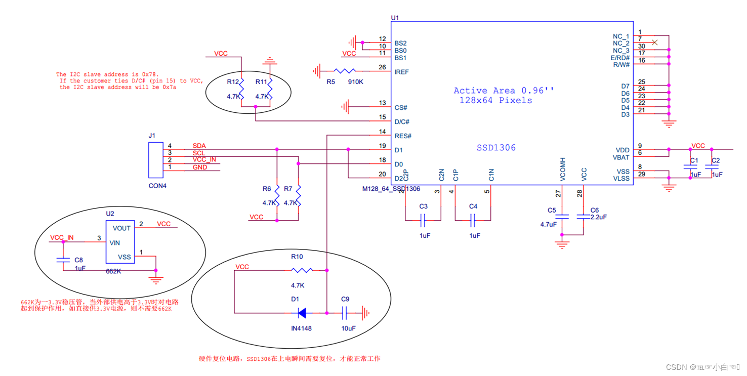
2.3 4针脚I2C接口模块原理图
2.4 通信时序
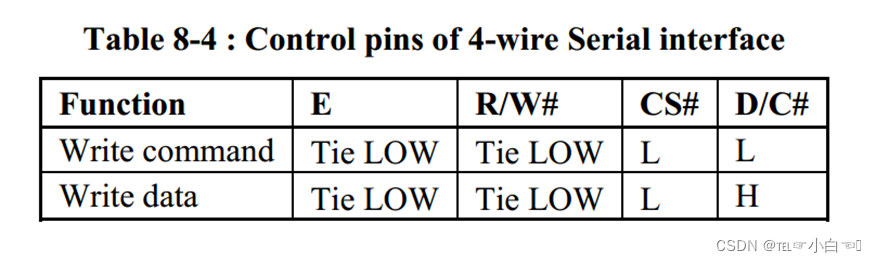
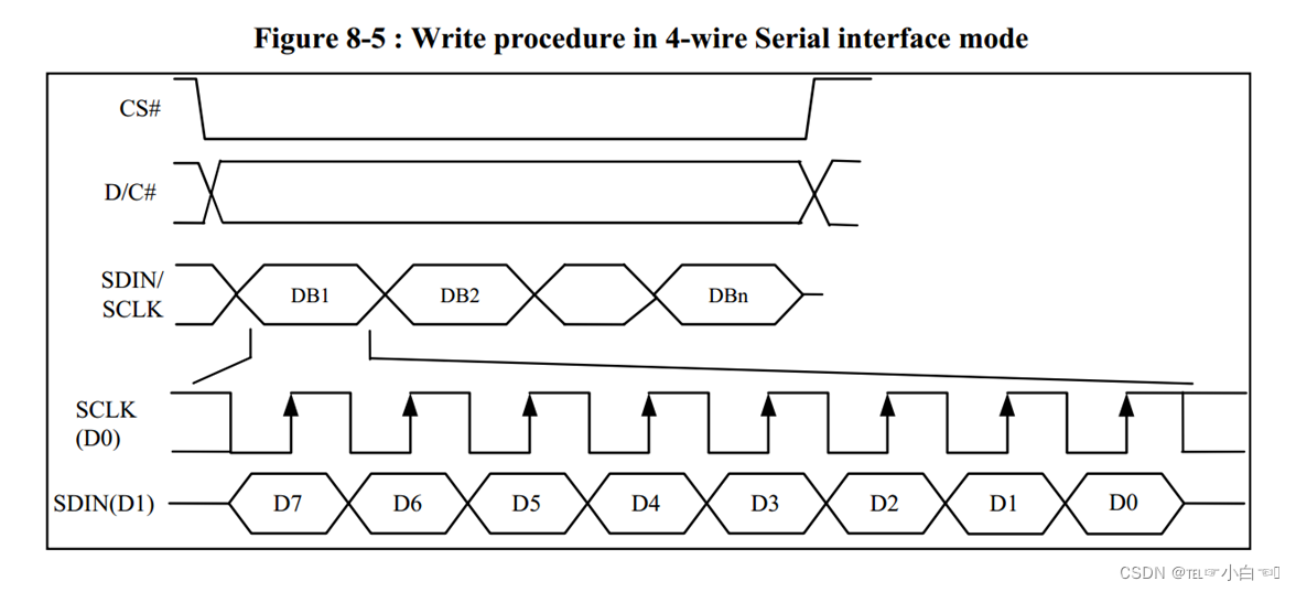
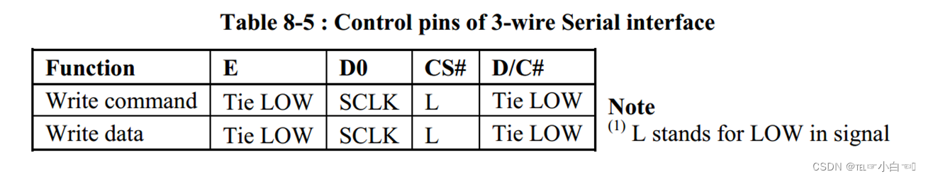
2.4.1 4线SPI的传输时序
串行传输只允许写,不允许读。因此,只有两个功能:写命令、写数据
E和R/W#时钟没用到,接低电平,CS#片选接低电平,表示始终选中此芯片
D/C#:高电平:数据,低电平:命令
2.4.2 3线SPI的传输时序

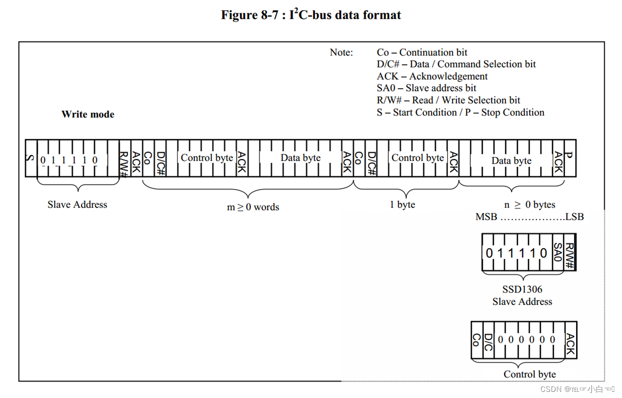
2.4.3 I2C的通信时序
Co(连续模式位):Co = 1,每发送一个字节数据前都加一个Control byte(命令和数据可以灵活切换)
Co = 0,在字节数据前只发送一个Control byte,之后全部都是字节数据
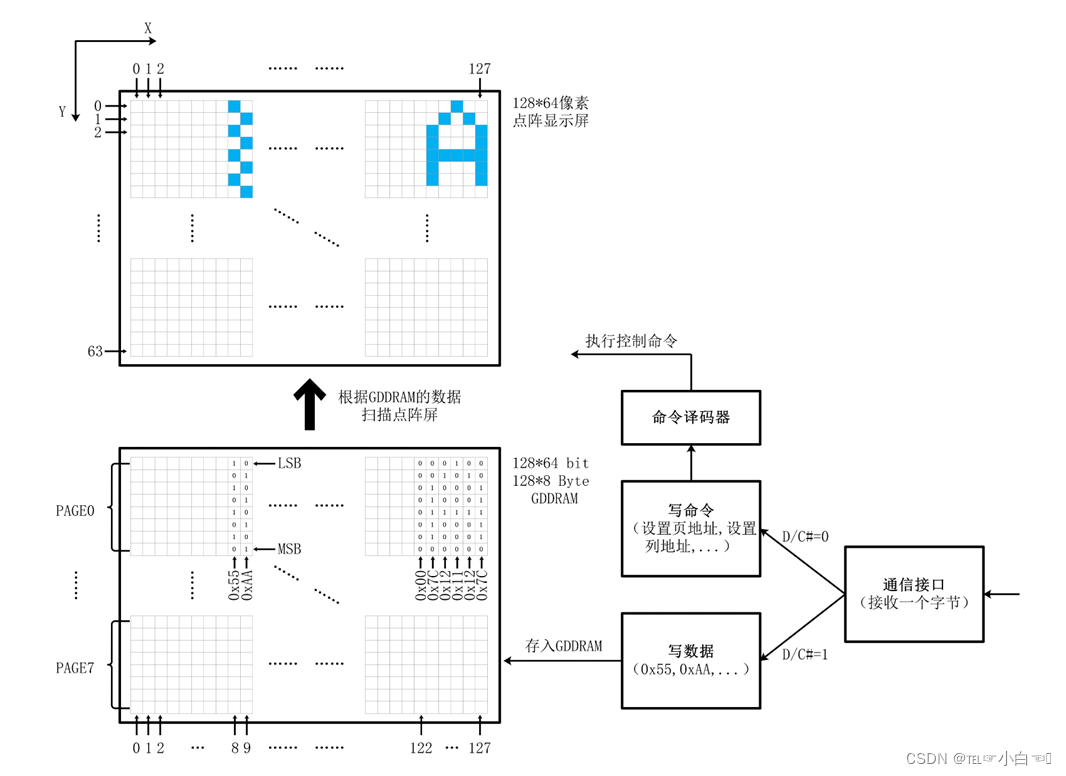
2.5 执行逻辑框图
左上角:128*64bit像素的点阵显示屏,以左上角为原点,向右为x正轴(0~127),向下为y正轴(0~63)
左下角:128*8Byte的GDDRAM,x轴与点阵显示屏一样,y轴有所不同,8位一组分为一页,范围为PAGE0 ~ PAGE7,共8页。每传输一个字节数据,将其展开,纵向排列(LSB在上,MSB在下),一位控制一个像素点
每写完一个字节数据后,内部的地址指针自动向右移动一个单位。当写到页的最后一字节时,地址指针默认回到页的起始位置,也可以通过配置寻址模式实现自动换页,换到下一页的开头
如果想要实现Y坐标的任意指定,需要读取GGDRAM,但串行传输只允许写数据,那需要在程序中定义缓存数组来实现:先读写缓存数组,最后一起更新到屏幕的GDDRAM中
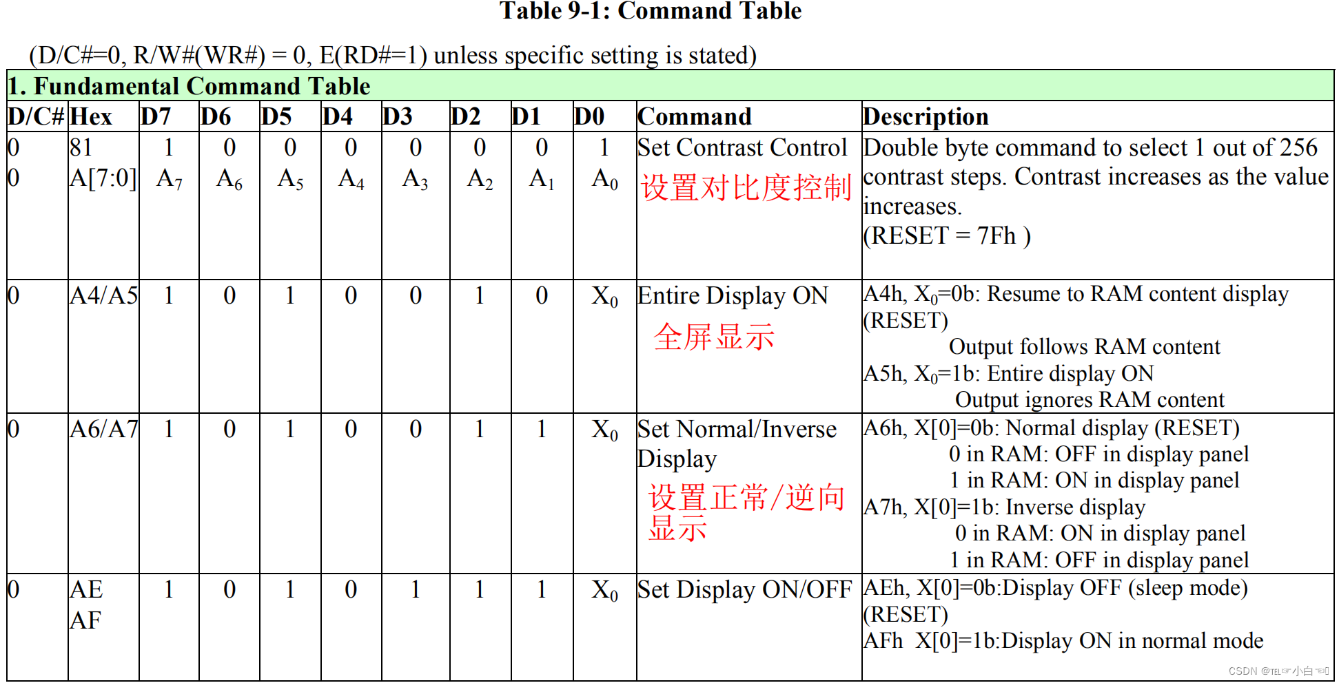
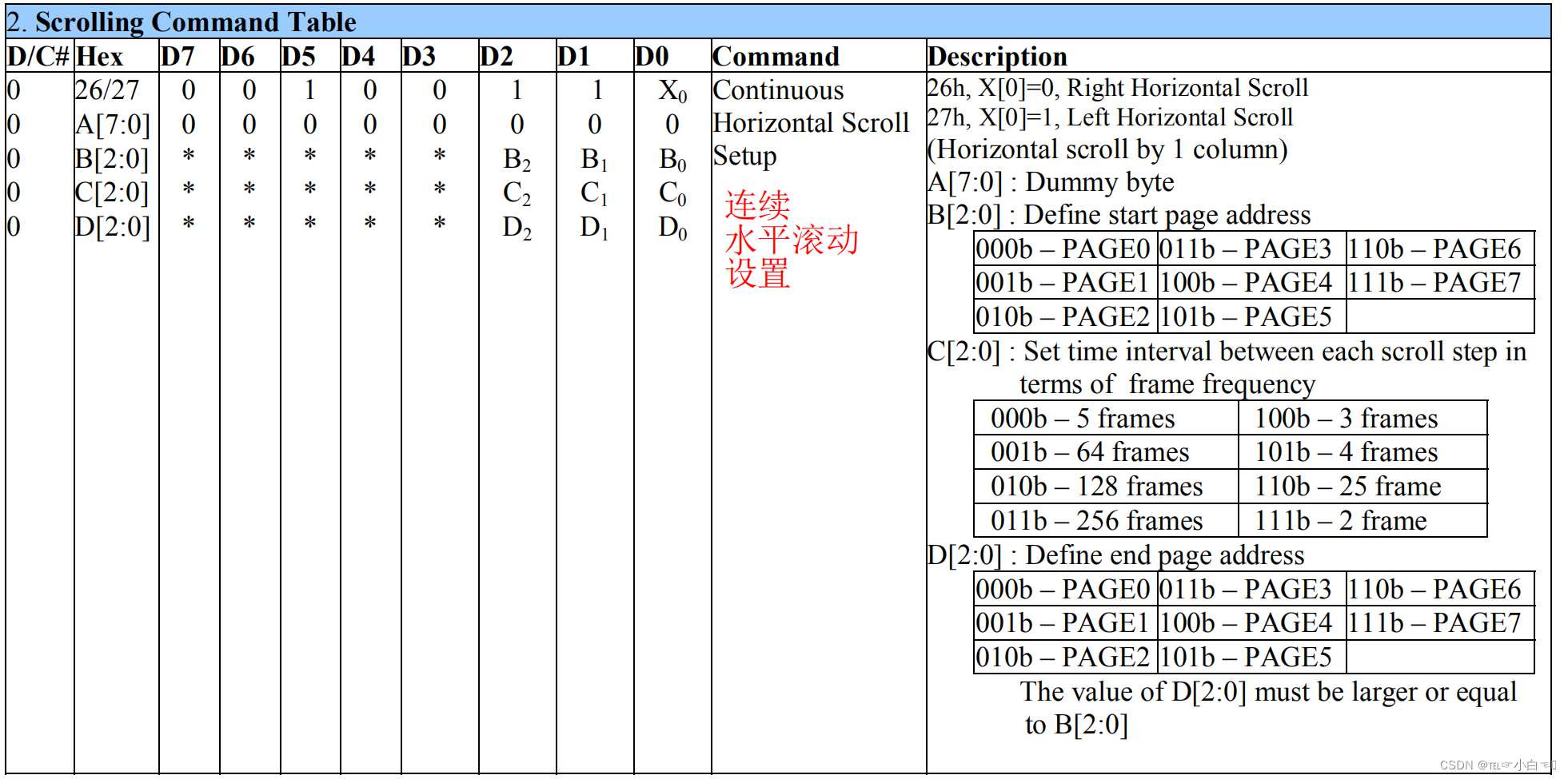
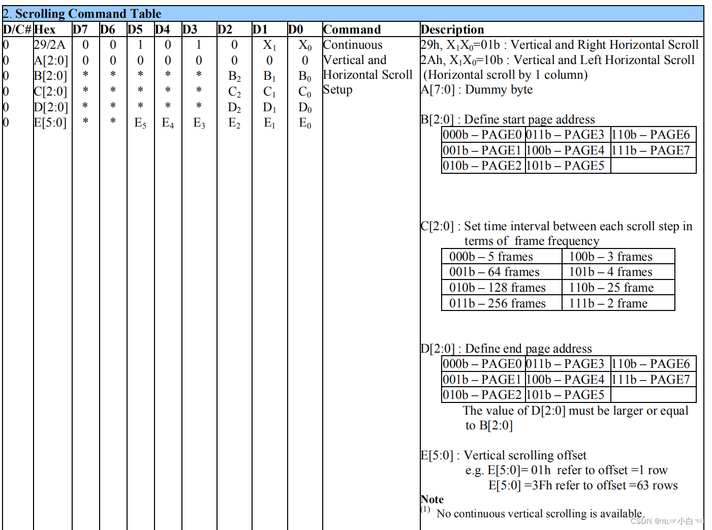
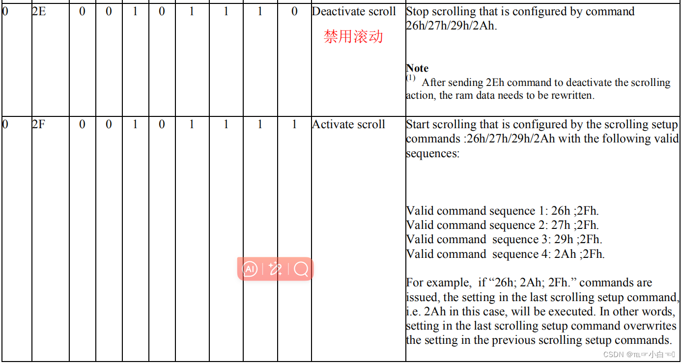
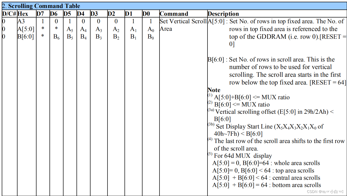
2.6 命令表
通过写命令时序传输的字节,作为发送给SSD1306的一个命令
SSD1306查询命令表的定义,执行相应的操作,命令可以由一个字节或者连续的多个字节组成
命令可分为基础命令、滚屏命令、寻址命令、硬件配置命令、时间及驱动命令5大类
2.6.1 基本命令表
2.6.2 滚动命令表
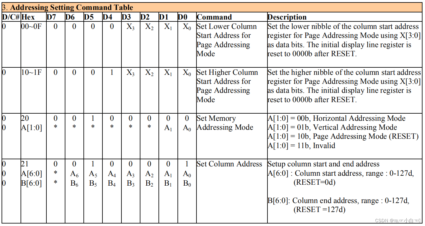
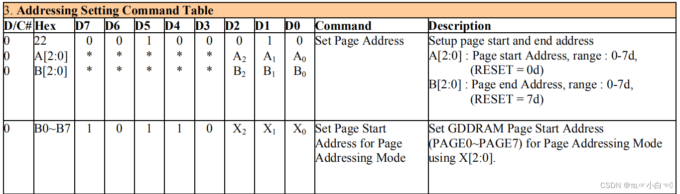
2.6.3 寻址设置命令表
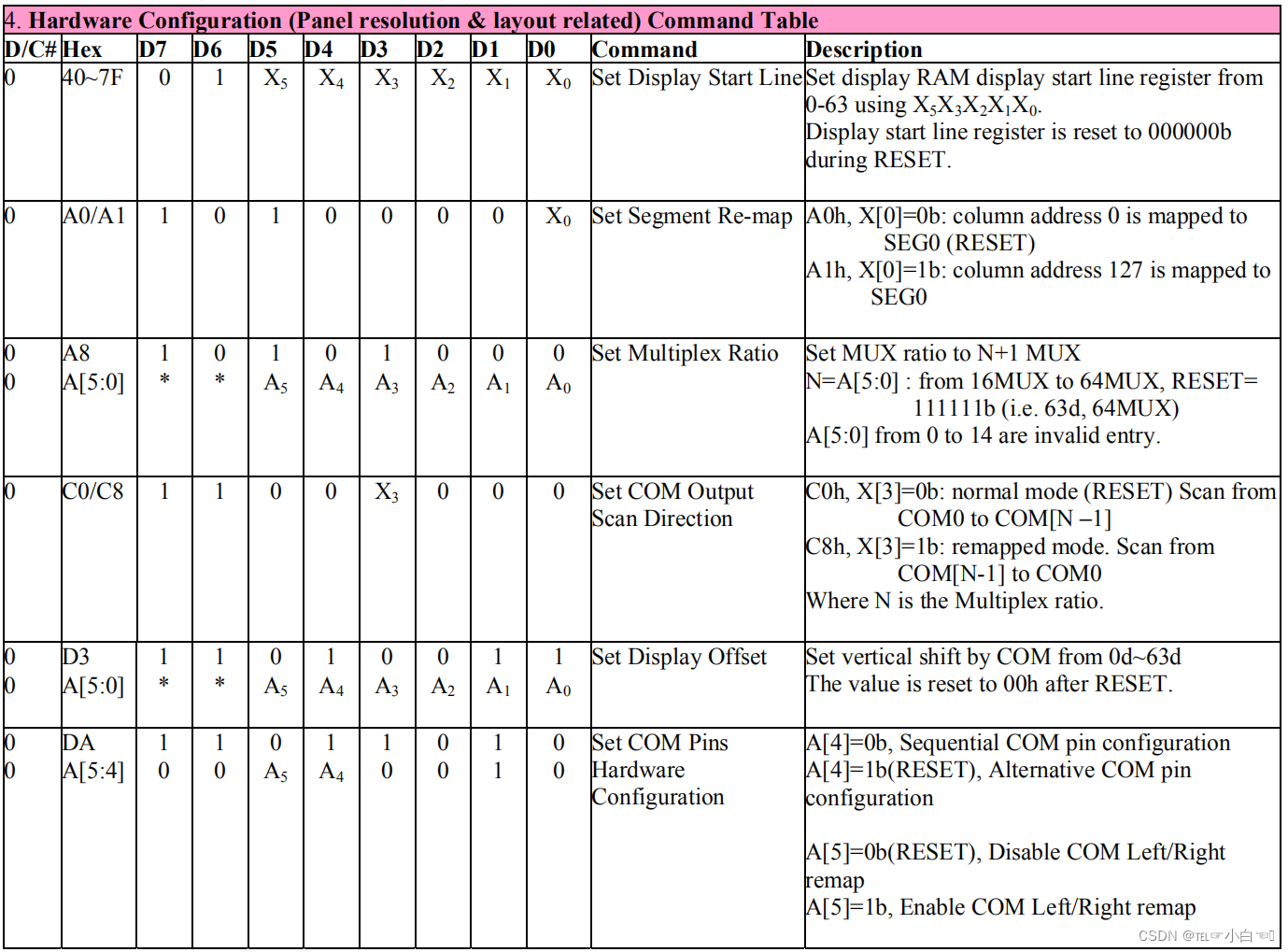
2.6.4 硬件配置命令表
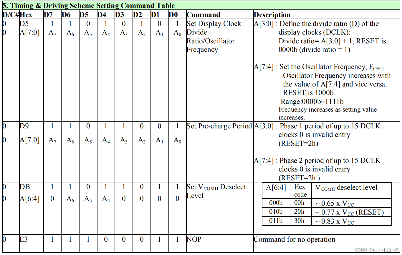
2.6.5 时间及驱动命令
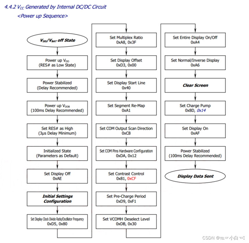
2.7 初始化过程(内部提供VCC)


 2704
2704

 被折叠的 条评论
为什么被折叠?
被折叠的 条评论
为什么被折叠?
 到【灌水乐园】发言


