差分阻抗90Ω±10%或者其他分别走什么阻抗

普通走线阻抗

必须选择 PCB 走线阻抗来匹配使用中的所有逻辑系别的特性阻抗(对于 CMOS 和 TTL,特性阻抗的范围是 80~110)。为了最好地将信号从源传送到负载,走线阻抗必须匹配发送设备的输出阻抗和接收设备的输入阻抗。

阻抗控制技术包括两个含义:
(1)阻抗控制的 PCB信号线是指沿高速 PCB 信号线各处阻抗连续,也就是说同一个网络上阻抗是一个常数。
(2)阻抗控制的 PCB 板是指 PCB 板上所有网络的阻抗都控制在一定的范围内,如20~75Ω。

线路板成为“可控阻抗板”的关键是使所有线路的特性阻抗满足一个规定值,通常在25~70Ω,一般取 50Ω。在多层线路板中,传输线性能良好的关键是使它的特性阻抗在整条线路中保持恒定。

HDMI接口布线要求

尽可能使 HDML连接器和器件之问的电气长度保持最短,从而使衰减最小化。为了使差分信号正常传输,一个差分对的两走线间距必须在整个走线轨迹上保持一致。否则,间距变化就会引起磁场耦合不平衡,从而降低磁场消除的效果,造成 EMI增加。推荐线宽间距比为1:1<W:S<1:2(W表示线宽,S 表示间距),差分线的线宽线距比如下图所示。HDMI差分走线控制阻抗要求是 100Ω,在计算阻抗的时候尽量按照此线宽间距比来进行。

差分等长、四对差分对之间的误差控制在 10mil 以内,每一对差分对对内之间的误差制在5mil之内,需要对单根走线进行绕线处理。PCB 设计的目的在于尽量将非连续性阳最小化。从而消除反射并保持信号完整。

可能发生非连续性的位置为:
(1)HDMI连接器焊盘同信号线迹相遇处;
(2)信号线迹碰到过孔、电阻器组件盘或IC引脚处;
(3)信号对被分离以围绕一个物体布线的地方,信号线的匹配电阻起防 ESD 作用和微调阻抗用途,通常靠近插座放置,但是两个电阻必须并排放置。

USB接口布线要求

(1)USB 差分走线越短越好,综合布局及结构进行调整。
(2)DP/DM 90Q差分走线,严格遵循差分走线规则,对内误差满足5mil。
(3)为抑制电磁辐射,USB 建议在内层走线,并保证走线参考面是一个连续完整的多考面,不被分割,否则会造成差分线阻抗的不连续性,并增加外部噪声对差分线的影响。穷间充足的情况下进行包地处理。同时尽量减少换层过孔,过孔会造成线路阻抗的不连续,实在需要的时候,建议在打孔换层处放置 GND 过孔。
(4)ESD保护器件、共模电感和大电容在布局时应尽可能地靠近 USB 接口摆放,线先通过静电器件及共模电感之后再进去接口。
(5)USB2.0规范定义的电流为500mA,但是VBUS走线最好能承受1A 的电流,以防过流。在使用 USB 充电的情况下,VBUS 走线需能承受 2.5A 的电流。

网口接口布线要求

MCU到网口芯片的走线,需进行等长控制,误差为 50mil。需进行阻抗控制,阻抗为50Ω。也应使其有完整的电源作为参考平面。
网口芯片到变压器及变压器到RJ45的信号为差分,一对 TX、一对 RX。阻抗控制为100Ω。需做对内等长,误差为5mil。
变压器在 PCB的投影区域内禁布器件和走线,电源层和地层需挖空。

LCD 接口布线要求

信号线需要做50Ω的阻抗控制。
应避免跨分割,注意不要从产生干扰的下方区域穿线。
总线有时序要求,需要进行等长控制,误差为50mil。
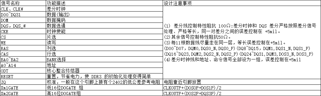
DDR3关键信号处理要点

在这里插入图片描述

Just when you thought you had mastered Zo, the characteristic impedance of a PCB trace, along comes a data sheet that tells you to design for a specific differential impedance. And to make things tougher, it says things like: “… since the coupling of two traces can lower the effective impedance, use 50 Ohm design rules to achieve a differential impedance of approximately 80 Ohms!” Is that confusing or what!! This article shows you what differential impedance is. But more than that, it discusses why it is, and shows you how to make the correct calculations. Single Trace: Figure 1(a) illustrates a typical, individual trace. It has a characteristic impedance, Zo, and carries a current, i. The voltage along it, at any point, is (from Ohm’s law) V = Zo*i. General case, trace pair: Figure 1(b) illustrates a pair of traces. Trace 1 has a characteristic impedance Z11, which corresponds to Zo, above, and current i1. Trace 2 is similarly defined. As we bring Trace 2 closer to Trace 1, current from Trace 2 begins to couple into Trace 1 with a proportionality constant, k. Similarly, Trace 1’s current, i1, begins to couple into Trace 2 with the same proportionality constant. The voltage on each trace, at any point, again from Ohm’s law, is: V1 = Z11 * i1 + Z11 * k * i2 Eqs. 1 V2 = Z22 * i2 + Z22 * k * i1 Now let’s define Z12 = k*Z11 and Z21 = k*Z22. Then, Eqs. 1 can be written as: V1 = Z11 * i1 + Z12 * i2 Eqs. 2 V2 = Z21 * i1 + Z22 * i2 This is the familiar pair of simultaneous equations we often see in texts. The equations can be generalized into an arbitrary number of traces, and they can be expressed in a matrix form that is familiar to many of you. Special case, differential pair: Figure 1(c) illustrates a differential pair of traces. Repeating Equations 1: V1 = Z11 * i1 + Z11 * k * i2 Eqs. 1 V2 = Z22 * i2 + Z22 * k * i1 Now, note that in a carefully designed and balanced situation, Z11 = Z22 = Zo, and i2 = -i1 This leads (with a little manipulation) to: V1 = Zo * i1 * (1-k)
评论
添加红包

请填写红包祝福语或标题

红包个数最小为10个

红包金额最低5元

当前余额3.43前往充值 >
需支付:10.00
成就一亿技术人!
领取后你会自动成为博主和红包主的粉丝 规则
hope_wisdom
发出的红包

打赏作者

谢谢~谢先生

你的鼓励将是我创作的最大动力

¥1 ¥2 ¥4 ¥6 ¥10 ¥20
扫码支付:¥1
获取中
扫码支付

您的余额不足,请更换扫码支付或充值

打赏作者

实付
使用余额支付
点击重新获取
扫码支付
钱包余额 0

抵扣说明:

1.余额是钱包充值的虚拟货币,按照1:1的比例进行支付金额的抵扣。
2.余额无法直接购买下载,可以购买VIP、付费专栏及课程。

余额充值