


- 双重平衡混频器
- 低失真:
+24 dBm三阶交调截点(IP3)
+10 dBm 1 dB压缩点 - 带宽:
500 MHz RF和LO输入带宽
250 MHz差分电流IF输出
直流到200 MHz以上单端电压IF输出 - 低LO驱动要求:–10 dBm
- 单电源或双电源供电
- 使用双电源时为直流耦合
所有端口都可直流耦合
无低频下限—工作频率低至DC - 用户可编程功耗
直接上图:


经测试,功能正常。
芯片说明
FEATURES
Doubly Balanced Mixer
Low Distortion
+24 dBm Third Order Intercept (IP3)
+10 dBm 1 dB Compression Point
Low LO Drive Required: –10 dBm
Bandwidth
500 MHz RF and LO Input Bandwidths
250 MHz Differential Current IF Output
DC to >200 MHz Single-Ended Voltage IF Output
Single- or Dual-Supply Operation
DC Coupled Using Dual Supplies
All Ports May Be DC Coupled
No Lower Frequency Limit—Operation to DC
User-Programmable Power Consumption
APPLICATIONS
High Performance RF/IF Mixer
Direct to Baseband Conversion
Image-Reject Mixers
I/Q Modulators and Demodulators
-------
特征
双平衡搅拌机
低失真
+24 dBm三阶截获(IP3)
+10 dBm 1 dB压缩点
所需低LO驱动:-10 dBm
带宽
500 MHz射频和本振输入带宽
250 MHz差分电流中频输出
直流至>200 MHz单端电压中频输出
单电源或双电源操作
使用双电源进行直流耦合
所有端口都可以直流耦合
无频率下限——直流运行
用户可编程功耗
应用
高性能RF/IF混频器
直接基带转换
图像拒绝混合器
I/Q调制器和解调器
PRODUCT DESCRIPTION
The AD83 1 is a low distortion, wide dynamic range, monolithic mixer for use in such applications as RF to IF downconversion in HF and VHF receivers, the second mixer in DMR base sta tions, direct-to-baseband conversion, quadrature modulation and demodulation, and doppler shift detection in ultrasound imaging applications. The mixer includes an LO driver and a low noise output amplifier and provides both user-programmable power consumption and third order intercept point.
The AD83 1 provides a +24 dBm third order intercept point for –1 0 dBm LO power, thus improving system performance and reducing system cost compared to passive mixers, by eliminating the need for a high power LO driver and its attendant shielding and isolation problems.
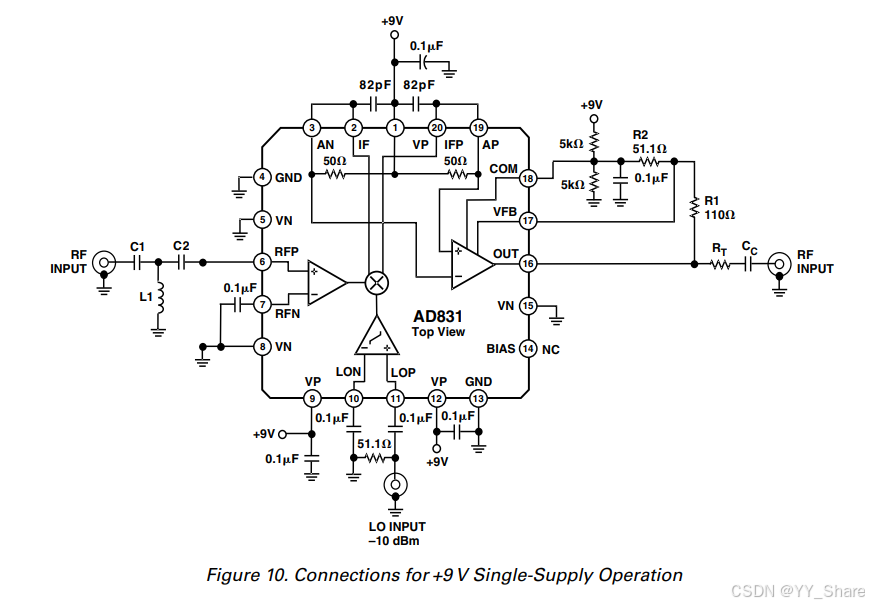
The RF, IF, and LO ports may be dc or ac coupled when the
mixer is operating from ±5 V supplies or ac coupled when oper ating from a single-supply of 9 V minimum. The mixer operates with RF and LO inputs as high as 500 MHz.
The mixer’s IF output is available as either a differential current output or a single-ended voltage output. The differential output is from a pair of open collectors and may be ac coupled via a trans former or capacitor to provide a 250 MHz output bandwidth. In downconversion applications, a single capacitor connected across these outputs implements a low-pass filter to reduce harmonics directly at the mixer core, simplifying output filtering. When
building a quadrature-amplitude modulator or image reject mixer, the differential current outputs of two AD83 1 s may be summed by connecting them together.
An integral low noise amplifier provides a single-ended voltage output and can drive such low impedance loads as filters, 50 amplifier inputs, and A/D converters. Its small signal bandwidth exceeds 200 MHz. A single resistor connected between pins OUT and FB sets its gain. The amplifier’s low dc offset allows its use in such direct-coupled applications as direct-to-baseband conversion and quadrature-amplitude demodulation. The mixer’s SSB noise figure is 1 0.3 dB at 70 MHz using its output amplifier and optimum source impedance. Unlike passive mixers, the AD83 1 has no insertion loss and does not require an external diplexer or passive termination.
A programmable-bias feature allows the user to reduce power
consumption, with a reduction in the 1 dB compression point and third-order intercept. This permits a tradeoff between dynamic range and power consumption. For example, the AD83 1 may be used as a second mixer in cellular and two-way radio base stations at reduced power while still providing a substantial performance
improvement over passive solutions
产品描述
AD83 1是一款低失真、宽动态范围的单片混频器,用于HF和VHF接收机中的RF到IF下变频、DMR基站中的第二混频器、直接到基带转换、正交调制和解调以及超声成像应用中的多普勒频移检测等应用。混频器包括LO驱动器和低噪声输出放大器,并提供用户可编程功耗和三阶截断点。
AD83 1为-1 0 dBm LO功率提供了+24 dBm的三阶截获点,从而通过消除对高功率LO驱动器的需求及其随之而来的屏蔽和隔离问题,与无源混频器相比,提高了系统性能并降低了系统成本。
当发生以下情况时,RF、IF和LO端口可以是直流或交流耦合
混合器在±5 V电源下运行,或在最小9 V的单电源下运行时进行交流耦合。混频器的RF和LO输入高达500 MHz。
混频器的中频输出可作为差分电流输出或单端电压输出。差分输出来自一对开路集电极,可以通过变压器或电容器进行交流耦合,以提供250 MHz的输出带宽。在下变频应用中,连接在这些输出端的单个电容器实现了低通滤波器,直接在混频器核心减少谐波,简化了输出滤波
通过构建正交幅度调制器或镜像抑制混频器,可以将两个AD83 1秒的差分电流输出连接在一起求和。
集成低噪声放大器提供单端电压输出,可以驱动滤波器、50放大器输入和a/D转换器等低阻抗负载。其小信号带宽超过200 MHz。连接在引脚OUT和FB之间的单个电阻器设置其增益。放大器的低直流偏移允许其用于直接耦合应用,如直接到基带转换和正交幅度解调。使用其输出放大器和最佳源阻抗,混频器的SSB噪声系数在70 MHz时为1 0.3 dB。与无源混频器不同,AD83 1没有插入损耗,不需要外部双工器或无源终端。
可编程偏置功能允许用户降低功耗
功耗降低,1dB压缩点和三阶截距减少。这允许在动态范围和功耗之间进行权衡。例如,AD83 1可以在降低功率的同时用作蜂窝和双向无线电基站中的第二混频器,同时仍然提供可观的性能被动解决方案的改进。
PRODUCT HIGHLIGHTS
1. –1 0 dBm LO Drive for a +24 dBm Output Referred Third
Order Intercept Point
2. Single-Ended Voltage Output
3. High Port-to-Port Isolation
4. No Insertion Loss
5. Single- or Dual-Supply Operation
6. 1 0.3 dB Noise Figure REV. C
产品亮点
1. -10 dBm LO驱动器+24 dBm输出参考第三
订单截点
2. 单端电压输出
3. 高端口到端口隔离
4. 无插入损耗
5. 单或双电源操作
6. 10.3分贝噪音图
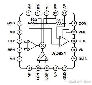
框图


 8015
8015

 被折叠的 条评论
为什么被折叠?
被折叠的 条评论
为什么被折叠?
 到【灌水乐园】发言


