


原理图
取n=14,这样总共会有16个晶体管,在版图时可以画成4x4矩阵,更好的匹配。
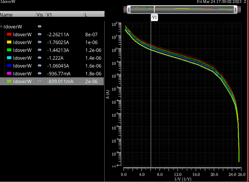
仿真PMOS晶体管
对单管pmos仿真gmid以及gain曲线
假设:gm/id=6,L=2u,Id=10uA
从gmid-id/w曲线中可以得到W=12u
bandgap中运放的设计
采用两级运放
假设CL=10p,GBW=50MHz,Av>10000

输入级pmos进行仿真
取Cc=CL/2=5p,根据 ,可以计算出gm1=2*10^-3
取gm/id=12,可以计算出id=167uA
Av>10000,每一级增益取100
Av1=gm1ro/2>100,需要gain>200
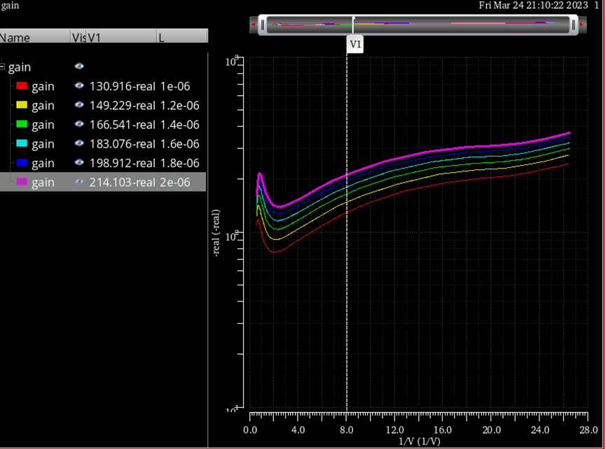
在gmid-gain中找到gain>200时的L
取L=400n
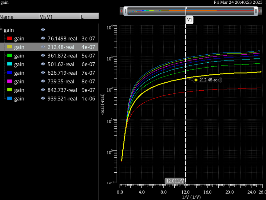
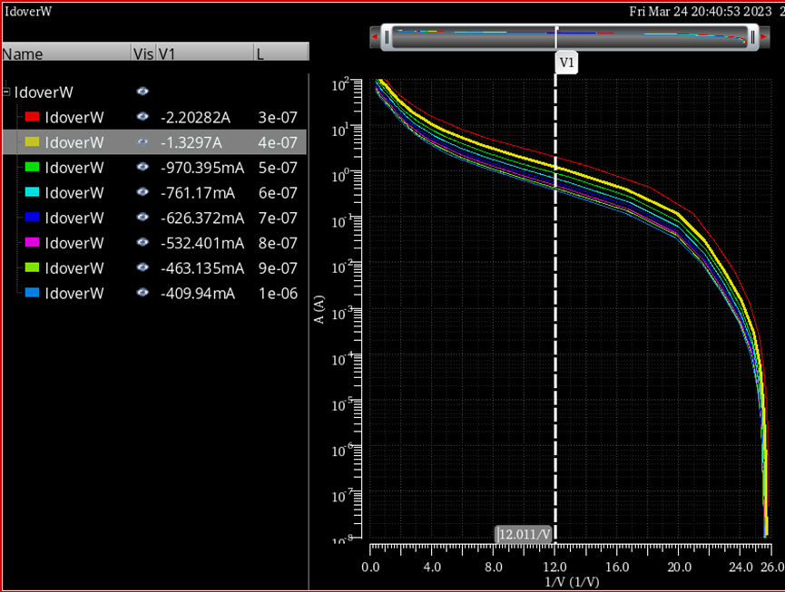
根据gmid-idw曲线求出W=121u,令m=4,W=31.5u
负载晶体管nmos仿真
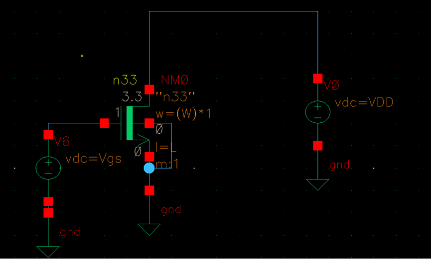
取gm/id=8,L=2u,W=145u,m=4时,w=36.56u

运放第二级nmos管仿真
确定晶体管M6的尺寸,晶体管M6的gm应为gm1的6倍,因此gm6=16*10^-3
取gm/id=8,id=2mA如图L=2u,同理从图中可以看出W=876u,取m=10,,w=87.6u
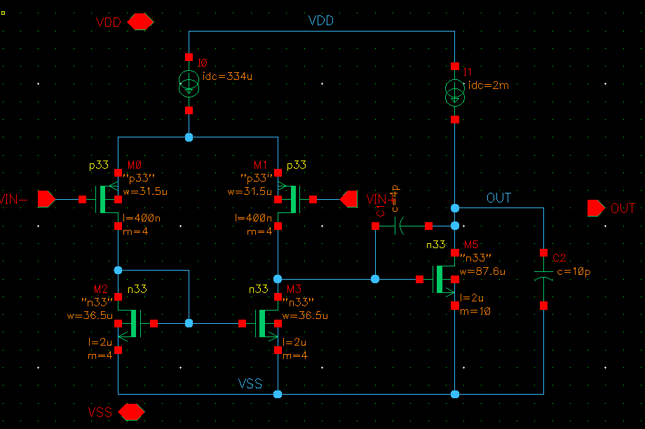
两级运放仿真


最后根据需求微调参数
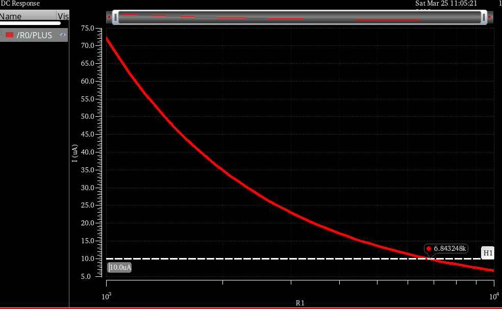
banggap仿真电阻R1,R2

假设支路电流为10uA,对R1进行扫描,取R1=6.85K
R2决定温度系数,对R2进行参数扫描,取R2=43k
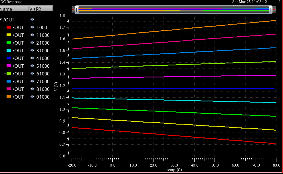
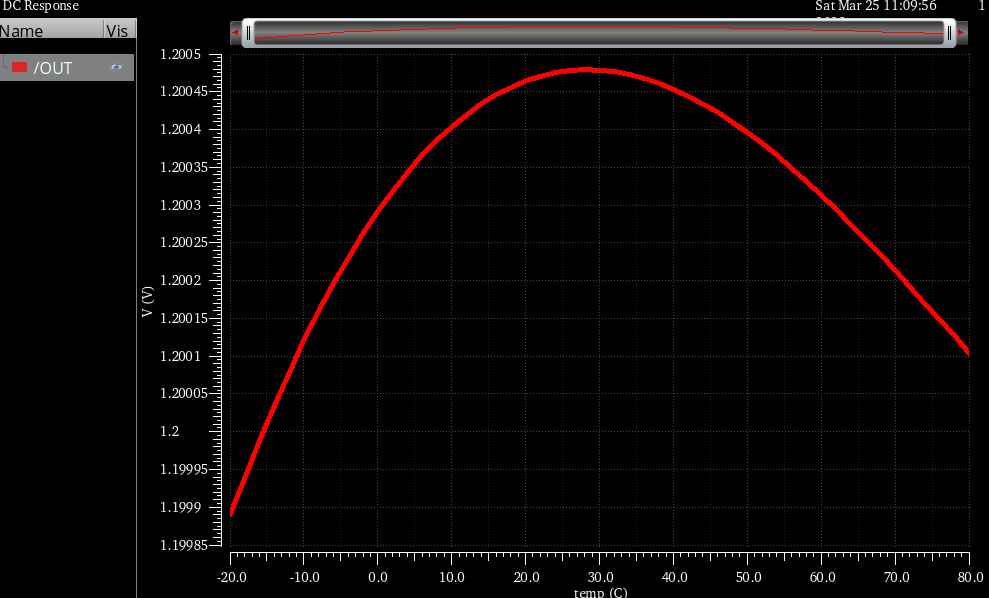
温度特性仿真
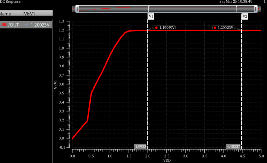
对VDD进行仿真


 1856
1856


 被折叠的 条评论
为什么被折叠?
被折叠的 条评论
为什么被折叠?
 到【灌水乐园】发言


