


SPI配置
SPI 时钟极性 和 相位
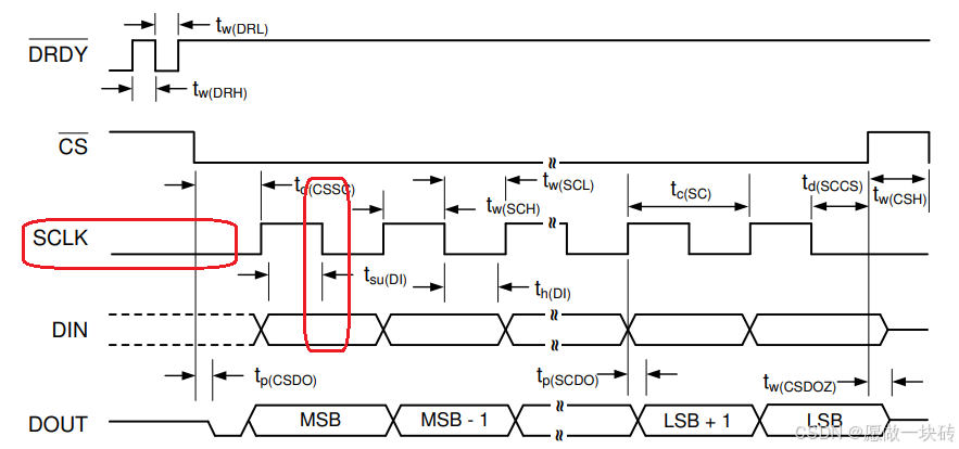
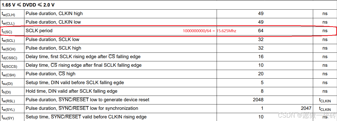
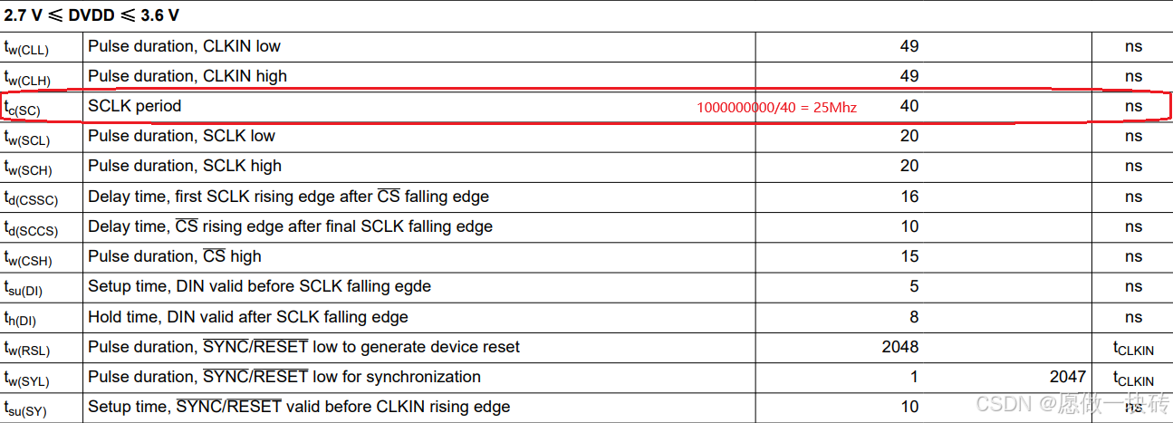
SPI SCK 频率
数据读取
SPI数据格式
An SPI communication frame with the ADS131M02 is made of words. Words on DIN can contain commands, register settings during a register write, or a CRC of the input data. Words on DOUT can contain command responses, register settings during a register read, ADC conversion data, or CRC of the output data.
Words can be 16, 24, or 32 bits. The word size is configured by the WLENGTH[1:0] bits in the MODE register. The device defaults to a 24-bit word size. Commands, responses, CRC, and registers always contain 16 bits of actual data. These words are always most significant bit (MSB) aligned, and therefore the least significant bits (LSBs) are zero-padded to accommodate 24- or 32-bit word sizes. ADC conversion data are nominally 24 bits. The ADC truncates its eight LSBs when the device is configured for 16-bit communication. There are two options for 32-bit communication available for ADC data that are configured by the WLENGTH[1:0] bits in the MODE register. Either the ADC data can be LSB padded with zeros or the data can be MSB sign extended.
//SPI通讯中,每帧数据全部由word构成。 word可以通过寄存器WLENGTH[1:0]配置为16位,24位,32位。
//SPI通讯中,高位先行。
//ADC转换结果通常为24位。
数据读取时序
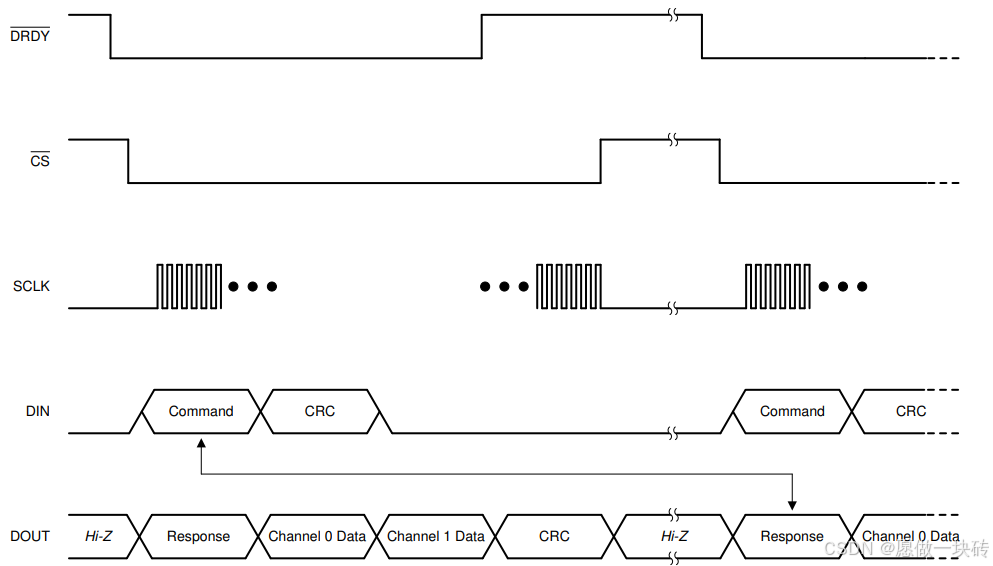 使用中断监控DRDY信号 DRDY信号低跳变表示转换完成,可以进行SPI通讯读取转换结果;
CS片选拉低;
SPI同步通讯发送命令并接收数据。
上图中Command,CRC,Response,Channel 0 Data, Channel 1 Data, CRC 均为24 bits (SPI 需要3 bytes的 SCK ).
ADC数据解析
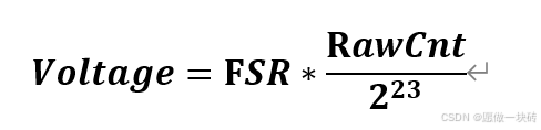
其中:
Voltage : 转换后得到的电压数值。
FSR: 选择的满偏电压数值。
RawCnt: 通过SPI读回的ADC 原始counter 值,注意 ADC的原始counter是带符号位的,由此可得到正的电压输入或者负向的电压输入。
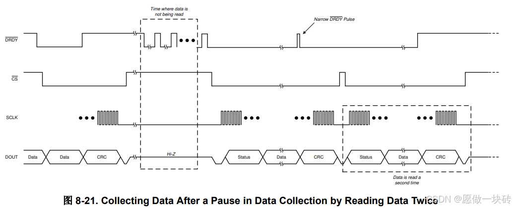
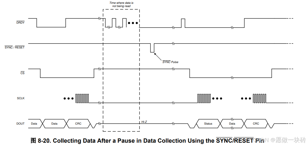
Narrow Pulse处理
当第一次读取AD 或者 AD的转换和读取速度不匹配时,DRDY信号会出现假的转换完成信号(负跳变),此时的转换数据不能被用来进行电压计算。
解决办法:
初次检测到DRDY负跳变,连续阻塞读取两次。或者检测到narrow pulse 后,通过RESET复位ADS131M0X芯片。
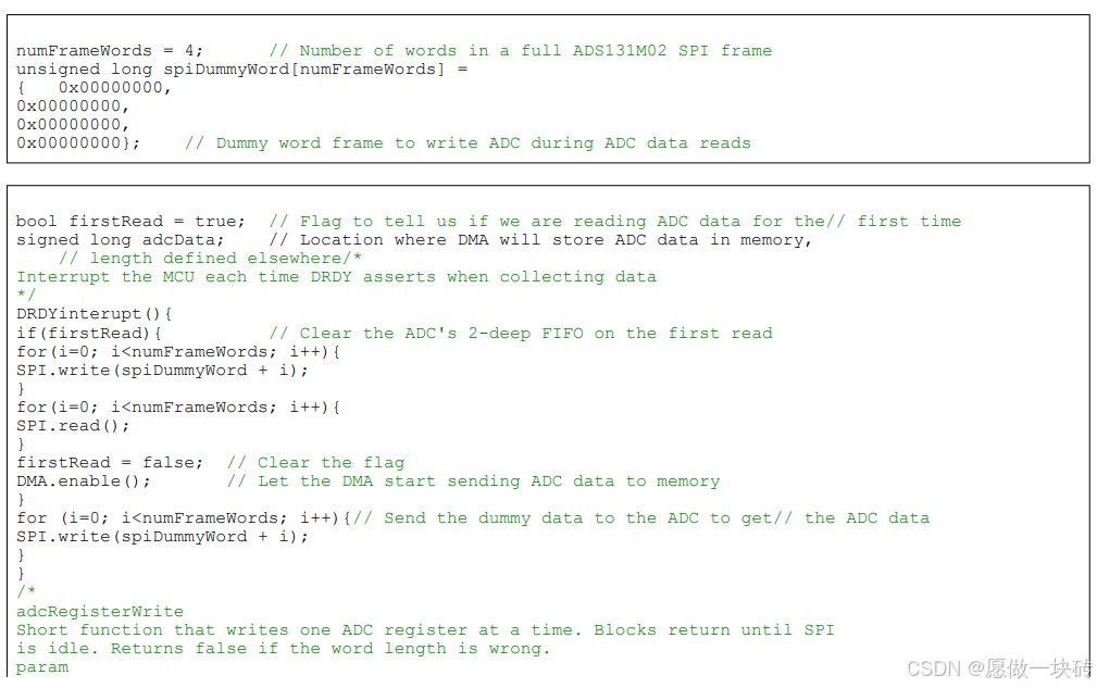
TI手册代码
AD校准
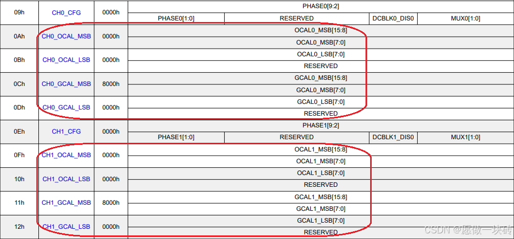
校准寄存器
OFFSET校准计算
The offset calibration registers are used to correct for system offset error, otherwise known as zero error. Offset error corresponds to the ADC output when the input to the system is zero. The ADS131M02 corrects for offset errors by subtracting the contents of the OCALn[23:0] register bits in the CHn_OCAL_MSB and CHn_OCAL_LSB registers from the conversion result for that channel before being output. There are separate CHn_OCAL_MSB and CHnOCAL_LSB registers for each channel, which allows separate offset calibration coefficients to be programmed for each channel. The contents of the OCALn[23:0] bits are interpreted by the device as 24-bit two's complement values, which is the same format as the ADC data.
//CHn_OCAL_MSB and CHn_OCAL_LSB组成的24bit数据为offset数值;
//AD转换完成后会自动减去CHn_OCAL_MSB and CHn_OCAL_LSB组成的24bit数据,此为offset校准。
//CHn_OCAL_MSB and CHn_OCAL_LSB组成的24bit数据 可正可负,数据格式和ADC数据格式形同。
GAIN校准计算
The gain calibration registers are used to correct for system gain error. Gain error corresponds to the deviation of gain of the system from its ideal value. The ADS131M02 corrects for gain errors by multiplying the ADC conversion result by the value given by the contents of the GCALn[23:0] register bits in the CHn_GCAL_MSB and CHn_GCAL_LSB registers before being output. There are separate CHn_GCAL_MSB and CHn_GCAL_LSB registers for each channel, which allows separate gain calibration coefficients to be programmed for each channel. The contents of the GCALn[23:0] bits are interpreted by the device as 24-bit unsigned values corresponding to linear steps ranging from gains of 0 to 2 – (1 / 223).
//CHn_GCAL_MSB and CHn_GCAL_LSB组成的24bit数据为GAIN标定校准数据。
//AD转换完成后会自动乘CHn_GCAL_MSB and CHn_GCAL_LSB组成的24bit数据,此为GAIN校准。


 2万+
2万+

 被折叠的 条评论
为什么被折叠?
被折叠的 条评论
为什么被折叠?
 到【灌水乐园】发言


