


关于DDS具体理论可以查看我的上一篇博客
https://blog.csdn.net/weixin_45614076/article/details/124973803?spm=1001.2014.3001.5501
首先生成相关的波形文件 coe
%generate sim wave data in the coe file
clear all;
clc;
rom_depth = 4096;
rom_width = 8;
y = zeros(rom_depth, 1);
for i = 1 : rom_depth
    y(i,1) = ceil((2^(rom_width-1) - 1) * sin(i/rom_depth * 2 * pi)) + 2^(rom_width -1) - 1;
end
plot(y);
fid = fopen('sin_wave.coe', 'wt');
fprintf(fid, "MEMORY_INITIALIZATION_RADIX = 10;\n");
fprintf(fid, 'MEMORY_INITIALIZATION_VECTOR =\n');
for i = 1 : rom_depth
    fprintf(fid, '%d ,\n', y(i,1));
end
接下来就是写verilog了,写呀写
module DDS_my(
        input   wire    [31:0]      Fword       ,
        input   wire                sys_clk     ,
        input   wire                rst_n       ,
        input   wire    [11:0]      Pword       ,

        output  wire    [7:0]      data_out
    );

    /* sync the Fword  */
    reg     [31:0]      Fword_sync;

    always @(posedge sys_clk or negedge rst_n) begin
        if(!rst_n)
            Fword_sync <= 32'd0;
        else
            Fword_sync <= Fword;
    end

    /* Acc the frequency */
    reg     [31:0]      Fword_ADD;

    always @(posedge sys_clk or negedge rst_n)
        if(!rst_n)
            Fword_ADD <= 32'd0;
        else
            Fword_ADD <= Fword_ADD + Fword_sync;

    /*note: the rom depth is 4096, bits needed are 12,
    so, Fword[31:20] cam be used to be an index. To explain
    in another way, when the Fword is set to 2^20, then step by step*/

    /* generate the index of ROM, Pword is added */

    reg     [11:0]      rom_index       ;
    always @(posedge sys_clk or negedge rst_n)
        if(!rst_n)
            rom_index <= 12'd0;
        else
            rom_index <= Fword_ADD[31:20] + Pword;

    /* instnce the rom ip */
    sin_rom u_sin_rom(
        .a  (rom_index )  ,
        .spo(data_out)
    );

endmodule
ROM ip核的创建 就不在这里说了
接下来写testbench
module tb_sin_wave();
`define PERIOD 20

reg     [31:0]      Fword   ;
reg                 sys_clk ;
reg                 rst_n   ;
reg     [11:0]      Pword   ;

wire    [7:0]      data_out;

initial begin
    sys_clk = 1'b0;
    rst_n = 1'b0;
    Fword = 2097152;
    Pword = 0;
    #30
    rst_n = 1'b1;
end

always #(`PERIOD) sys_clk = ~sys_clk;

DDS_my      u_DDS_my(
        .   Fword    (Fword)    ,
        .   sys_clk  (sys_clk)  ,
        .   rst_n    (rst_n)    ,
        .   Pword    (Pword)    ,

        .   data_out  (data_out)
    );

endmodule
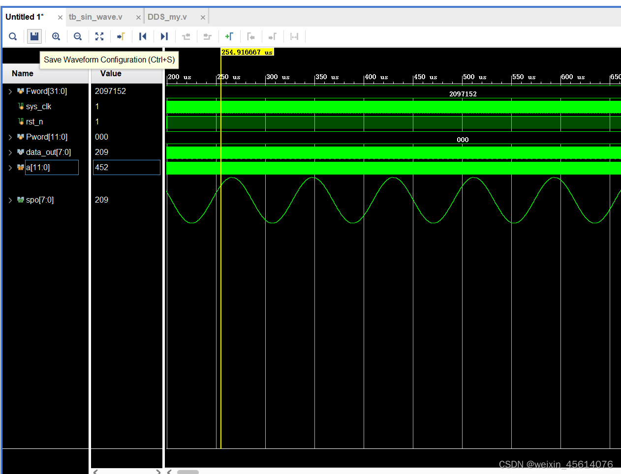
最后就是仿真波形了
一名FPGA 爱好学习者,继续努力!!!!


 3928
3928


 被折叠的 条评论
为什么被折叠?
被折叠的 条评论
为什么被折叠?
 到【灌水乐园】发言


