


HDLBits刷题笔记
Step one
Build a circuit with no inputs and one output. That output should always drive 1 (or logic high).
Solution:
module top_module( output one );
// Insert your code here
assign one = 1;
endmodule
Zero
Build a circuit with no inputs and one output that outputs a constant 0
Solution:
module top_module(
output zero
);// Module body starts after semicolon
assign zero = 1'b0;
endmodule
Wire
Create a module with one input and one output that behaves like a wire.

Solution:
module top_module( input in, output out );
assign out = in;
endmodule
Wire4
Create a module with 3 inputs and 4 outputs that behaves like wires that makes these connections:
a -> w
b -> x
b -> y
c -> z

Solution:
module top_module(
input a,b,c,
output w,x,y,z );
assign w = a;
assign x = b;
assign y = b;
assign z = c;
endmodule
Notgate
Create a module that implements a NOT gate.创建非门inverter (or "NOT-gate")

Solution:
module top_module( input in, output out );
assign out = !in;
endmodule
Andgate
Create a module that implements an AND gate.与门

Solution:
module top_module(
input a,
input b,
output out );
assign out = a & b;
endmodule
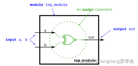
Norgate
Create a module that implements a NOR gate. A NOR gate is an OR gate with its output inverted. A NOR function needs two operators when written in Verilog.

Solution:
module top_module(
input a,
input b,
output out );
assign out = a | b;
endmodule
Xnorgate
Create a module that implements an XNOR gate.异或非门
Solution:
module top_module(
input a,
input b,
output out );
assign out = ~(a ^ b);
endmodule
Declaring wires
Implement the following circuit. Create two intermediate wires (named anything you want) to connect the AND and OR gates together. Note that the wire that feeds the NOT gate is really wire out, so you do not necessarily need to declare a third wire here.

Solution:
`default_nettype none
module top_module(
input a,
input b,
input c,
input d,
output out,
output out_n );
wire w1,w2;
assign w1 = a&b;
assign w2 = c&d;
assign out = w1 | w2;
assign out_n = ~(w1|w2);
endmodule
7458
The 7458 is a chip with four AND gates and two OR gates. This problem is slightly more complex than 7420. It has 10 inputs and 2 outputs. You may choose to use an assign statement to drive each of the output wires, or you may choose to declare (four) wires for use as intermediate signals, where each internal wire is driven by the output of one of the AND gates.

Solution:
module top_module (
input p1a, p1b, p1c, p1d, p1e, p1f,
output p1y,
input p2a, p2b, p2c, p2d,
output p2y );
wire w1,w2,w3,w4;
assign w1 = p1a&p1b&p1c;
assign w2 = p1d&p1e&p1f;
assign p1y = w1|w2;
assign w3 = p2a&p2b;
assign w4 = p2c&p2d;
assign p2y = w3|w4;
endmodule


 4316
4316


 被折叠的 条评论
为什么被折叠?
被折叠的 条评论
为什么被折叠?
 到【灌水乐园】发言


