


PCB Footprint Design Guidelines
Key Takeaways
The PCB footprint is the physical interface between the component and the circuit board.
The PCB footprint gives the designated locations to solder the components as per the design.
IPC-7351 is the standard that ensures the utmost solder joint quality after the placement of components.
It is important to follow PCB footprint design guidelines, as they ensure the circuit meets design criteria
The PCB footprint is the physical layout that represents the electrical and mechanical components of a board. The footprint comprises the arrangement of the metal pads, vias, through-holes, etc., and plays a critical role in ensuring the electrical and mechanical connections on the board. It is important to follow PCB footprint design guidelines, as they ensure the circuit meets design criteria and works properly. Let’s discuss the PCB footprint design guidelines that you should follow.
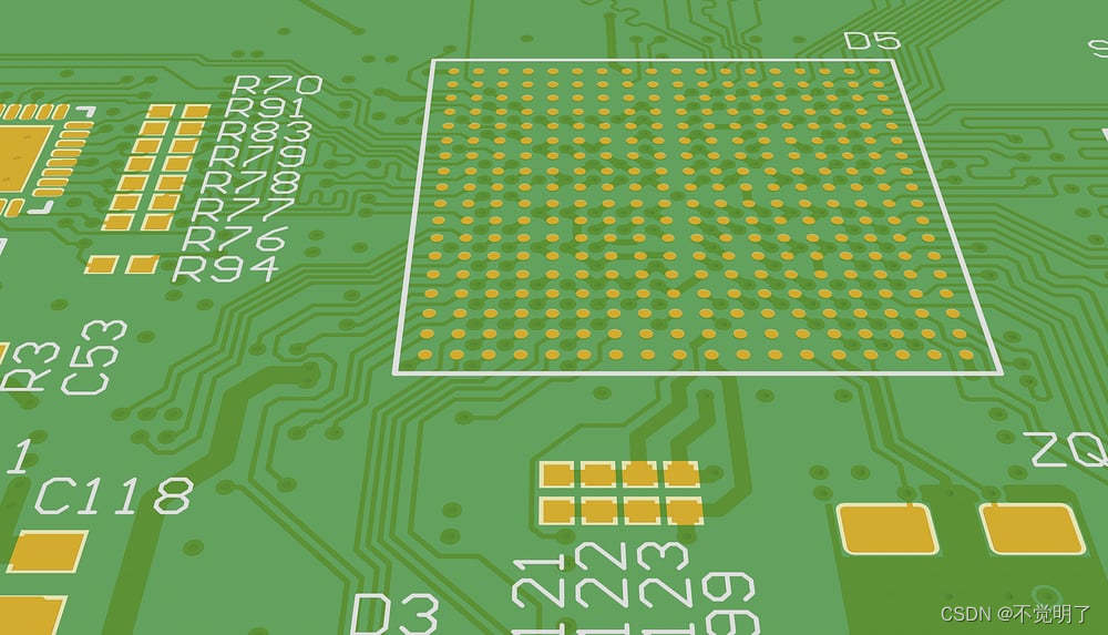
PCB Footprints

The PCB footprint gives the designated locations to solder the components as per the design as well as the physical size of the components, placement location, and associated traces. The PCB is then assembled according to the PCB footprint, also called a land pattern or pad pattern. Through traces and vias, the PCB footprints on a board are interconnected.
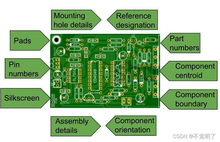
The Various Parts of a PCB Footprint
Standard Packages and PCB Footprints
For all standard components, footprints are available within the PCB design software library. However, there is a provision to create the PCB footprint by the designer as well. The PCB footprint should match the component in physical dimensions. Otherwise, they will not fit into the pads.
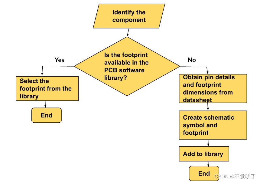
Creating PCB Footprints
Sometimes designers have to create their own PCB footprints. Imagine you are using a component in your circuit, but could not find the component library in the PCB design software database. This is an example of a time you might have to design your own PCB footprint. Other situations where you might create a PCB footprint include:
-When the manufacturer's datasheet does not provide the land pattern.
-When you are creating or using sub-assemblies consisting of components such as ICs, passive elements, or even combinations of multiple circuits.
The Steps to Creating a PCB Footprint
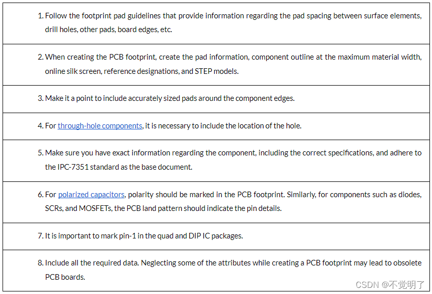
PCB Footprint Design Guidelines
PCB footprint design guidelines detail the arrangement of the pads and the distance between consecutive pads. The PCB footprint should clearly distinguish the component spacing, board edges, mounting holes, etc. Here are some common PCB footprint design guidelines:


 715
715

 被折叠的 条评论
为什么被折叠?
被折叠的 条评论
为什么被折叠?
 到【灌水乐园】发言


