


一、部分常用时钟原语介绍
1、
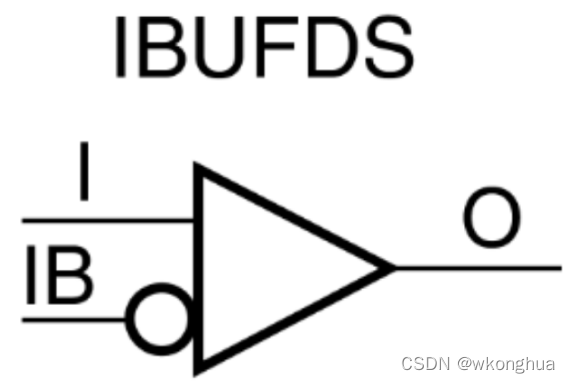
IBUFDS、OBUFDS:差分信号缓冲器,用于不同电平接口之间缓冲和转换。用于普通bank的差分时钟转单端。
1)、IBUFDS为差分输入缓冲器,支持低压差分信号LVCMOS、LVDS等:
| 端口 | IO | 位宽 | 功能 |
| I | input | 1 | 差分输入+ |
| IB | input | 1 | 差分输入- |
| O | output | 1 | 输出 |
| input | output | |
| I | IB | O |
| 0 | 0 | 不改变,和上次输出相同 |
| 0 | 1 | 0 |
| 1 | 0 | 1 |
| 1 | 1 | 不改变,和上次输出相同 |
// IBUFDS : In order to incorporate this function into the design,
// Verilog : the following instance declaration needs to be placed
// instance : in the body of the design code. The instance name
// declaration : (IBUFDS_inst) and/or the port declarations within the
// code : parenthesis may be changed to properly reference and
// : connect this function to the design. All inputs
// : and outputs must be connected.
// <-----Cut code below this line---->
// IBUFDS: Differential Input Buffer
// Virtex-7
// Xilinx HDL Language Template, version 2018.2
IBUFDS #(
.DIFF_TERM("FALSE"), // Differential Termination
.IBUF_LOW_PWR("TRUE"), // Low power="TRUE", Highest performance="FALSE"
.IOSTANDARD("DEFAULT") // Specify the input I/O standard
) IBUFDS_inst (
.O(O), // Buffer output
.I(I), // Diff_p buffer input (connect directly to top-level port)
.IB(IB) // Diff_n buffer input (connect directly to top-level port)
);
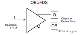
// End of IBUFDS_inst instantiation2)、 OBUFDS为查分数出缓冲器,用于将内部逻辑信号转换成差分信号输出,支持TMDS、LVDS等电平。
| 端口 | IO | 位宽 | 功能 |
| O | output | 1 | 差分输出+ |
| OB | output | 1 | 差分输出- |
| I | input | 1 | 输入 |
| input | output | |
| I | O | OB |
| 0 | 0 | 1 |
| 1 | 1 | 0 |
//     OBUFDS      : In order to incorporate this function into the design,
//     Verilog     : the following instance declaration needs to be placed
//    instance     : in the body of the design code.  The instance name
//   declaration   : (OBUFDS_inst) and/or the port declarations within the
//      code       : parenthesis may be changed to properly reference and
//                 : connect this function to the design.  Delete or comment
//                 : out inputs/outs that are not necessary.

//  <-----Cut code below this line---->

   // OBUFDS: Differential Output Buffer
   //         Artix-7
   // Xilinx HDL Language Template, version 2018.2

   OBUFDS #(
      .IOSTANDARD("DEFAULT"), // Specify the output I/O standard
      .SLEW("SLOW")           // Specify the output slew rate
   ) OBUFDS_inst (
      .O(O),     // Diff_p output (connect directly to top-level port)
      .OB(OB),   // Diff_n output (connect directly to top-level port)
      .I(I)      // Buffer input
   );

   // End of OBUFDS_inst instantiation
2、
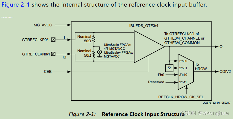
IBUFDS_GTEx,x=2/3/4,差分缓冲器,用于高速BANK(GTY BANK)的两路参考时钟输入。
其中UltraScale使用IBUFDS_GTE3作为GTY bank的差分缓冲器,UltraScale+采用IBUFDS_GTE4。对于高速BANK,需要使用IBUFDS_GTEx(不同系列的FPGA x的值不同,如x=2/3/4),如果仍然使用IBUFDS,可能会在编译或者生成bit文件时报错,提示时钟约束有问题,约束后可以生成bit文件,但是转出的单端时钟不能使用(正常情况下差分时钟的电平是不需要约束的)。
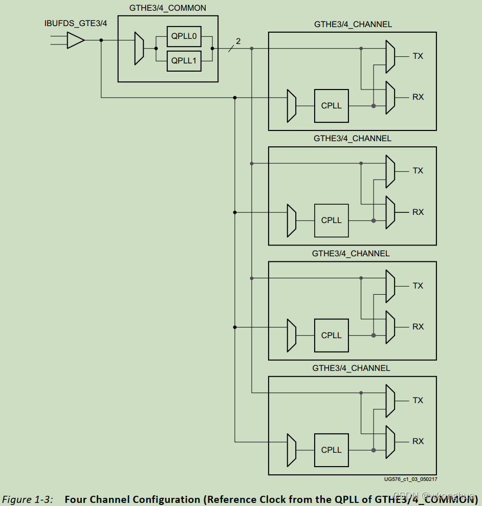
UltraScale架构中的GTY收发器是高速收发器,在UltraScale FPGA中支持500Mb/s到30.5Gb/s,在UltraScale+ FPGA中支持32.75Gb/s。每个GTY BANK包括四路收发通道,即一个QUAD,每个收发通道具有独立的通道锁相环CPLL,为收发数据提供参考时钟,每个QUAD还有两个共用的QPLL时钟资源可提供到四个收发通道。
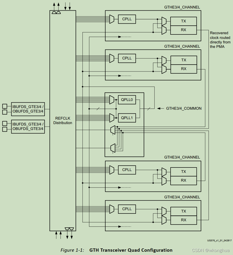
使用原语驱动GTX/GTH/GHY参考时钟,每个Quad有两个IBUFDS_GTEx元件,驱动GTREFCLK0和GTREFCLK1,常用模式是实例化一个IBUFDS_GTEx并驱动两个参考时钟之一。
// IBUFDS_GTE4 : In order to incorporate this function into the design,
//   Verilog   : the following instance declaration needs to be placed
//  instance   : in the body of the design code.  The instance name
// declaration : (IBUFDS_GTE4_inst) and/or the port declarations within the
//    code     : parenthesis may be changed to properly reference and
//             : connect this function to the design.  All inputs
//             : and outputs must be connected.

//  <-----Cut code below this line---->

   // IBUFDS_GTE4: Gigabit Transceiver Buffer
   //              Kintex UltraScale+
   // Xilinx HDL Language Template, version 2018.2

   IBUFDS_GTE4 #(
      .REFCLK_EN_TX_PATH(1'b0),   // Refer to Transceiver User Guide
      .REFCLK_HROW_CK_SEL(2'b00), // Refer to Transceiver User Guide
      .REFCLK_ICNTL_RX(2'b00)     // Refer to Transceiver User Guide
   )
   IBUFDS_GTE4_inst (
      .O(O),         // 1-bit output: Refer to Transceiver User Guide
      .ODIV2(ODIV2), // 1-bit output: Refer to Transceiver User Guide
      .CEB(CEB),     // 1-bit input: Refer to Transceiver User Guide
      .I(I),         // 1-bit input: Refer to Transceiver User Guide
      .IB(IB)        // 1-bit input: Refer to Transceiver User Guide
   );

   // End of IBUFDS_GTE4_inst instantiation
/// IBUFG/BUFG/......中'G'为Global Clock/General Clock?
3、
IBUFG即输入全局缓冲, 是与专用全局时钟输入管脚相连接的首级全局缓冲。所有从全局时钟管脚输入的信号必须经过IBUF单元,否则布局布线时会报错。IBUFG支持AGP、CTT、GTL、GTLP、HSTL、LVCMOS、LVDCI等多种格式的IO标准。
4、
BUFG是全局缓冲,它的输入是IBUFG的输出,BUFG的输出到达FPGA内部的IOB、CLB、RAM的时钟延迟和抖动最小。
5、
BUFGP相当于IBUFG + BUFG。
6、
BUFGCE是带有使能端的全局缓冲。有一个输入I、一个使能端CE、一个输出O,只有当BUFGCE使能端有效时,BUFGCE才有输出。
7、
BUFGMUX全局时钟选择缓冲,有I0和I1两个输入,一个控制端S,一个输出端口O。当S为低电平时输出时钟为I0,否则为I1。BUFGMUX使用灵活,I0和I1两个输入时钟可以是异步关系。
8、
BUFGDLL全局缓冲延迟锁相环,相当于BUFG+DLL的结合,在早期设计中经常使用,用以完成全局时钟同步和驱动等功能,随着数字时钟管理单元(DCM)的日益完善,目前BUFGDLL的应用已经逐渐被DCM替代。
9、
IBUFGDS/OBUFGDS(专用差分输入时钟缓冲器)是IBUFG/OBUFG的差分形式,当信号从一对差分全局时钟管脚输入时,必须使用IBUFGDS作为全局时钟输入缓冲。IBUFGDS实质上是一个连接时钟信号BUFG或DCM的专用的差分信号输入缓冲器,在IBUFGDS中一个电平接口用两个独立的电平接口(I和IB)表示,一个认为是主信号一个是从信号,相位相反。(7系列中没有找到?)
10、
DCM数字时钟管理单元,主要完成时钟同步、移相、分频、倍频、去抖等。DCM与全局时钟有着密不可分的联系,为达到最小延迟和抖动,几乎所有的DCM应用都要使用全局缓冲资源。DCM可以用xilinx ISE中的Architecture Wizard直接生成。
二、全局时钟资源使用方法
1、 IBUFG + BUFG
IBUFG后面连接BUFG,这种组合相当于BUFGP。
2、IBUFGDS + BUFG
当输入时钟信号为差分信号时,使用IBUFGDS代替IBUFG,即IBUFGDS + BUFG。
3、IBUFG + DCM + BUFG
这种灵活的方法对全局时钟的控制更加有效,通过DCM模块不仅能对时钟进行同步、移相、分频、倍频等,而且可以使全局时钟输出达到无抖动延迟。
参考:XILINX Ultrascale/Ultrascale+ 高速收发器时钟MGTHREFCLK原语调用_青豆哒哒的博客-CSDN博客
IBUFDS、IBUFGDS和OBUFDS_hi请叫我学霸的博客-CSDN博客_ibufds
BUFG、差分转单端之IBUFDS和IBUFDS_GTE2区别_朝阳群众&热心市民的博客-CSDN博客_ibufds_gte2
https://www.csdn.net/tags/OtDaIgzsNDYwMDMtYmxvZwO0O0OO0O0O.html
xilinx提供了丰富的原语,可以将之看成FPGA开发可以使用的库函数,原语在FPGA中具有与之对应的硬件逻辑单元,但也注意,不同的FPGA的原语可能会有所不同,但常用的原语不同器件相似度极高。按照功能,主要分为:计算组件、I/O端口组件、寄存器和锁存器、时钟组件、处理器组件、移位寄存器、配置和检测组件、RAM/ROM组件、Slice/CLB组件以及G比特组件。
选择时钟组件,对时钟组件的原语进行介绍,时钟组件包括各种全局时钟缓冲器、全局时钟复用器以及高级数字时钟管理模块,主要介绍前两个。
参考:
//-----------------------------------下一篇博客参考文章----------------------------------------


 9574
9574

 被折叠的 条评论
为什么被折叠?
被折叠的 条评论
为什么被折叠?
 到【灌水乐园】发言


