


自己动手写CPU【环境配置以及第一条ori指令】
一.前言
自己动手写cpu这本书是雷思磊所著。通过这本书,作者将带着我们从一个最简单的或指令情况出发,逐步搭建处一个功能完整的五级流水线结构,兼容MIPS32 release1指令集。从2022年十一月份开始利用了课程闲暇时间,将处理器软核部分复现完成。这个系列的博客主要是复盘一下这个过程。
我也在github上开源了相关代码,从第四章到第十一章,通过readme可以看见每个不同功能实现的具体代码。
源码:https://github.com/tongjiaxuan666/DIY_CPU

自己动手写cpu这本书通俗易懂,很容易复现。通过实践我们搭建一个简单的处理器模型,对计算机组成原理和体系结构的理解也大有益处。
二.环境配置
2.1 vcs+verdi
相信大家都用过Vivado,Quartus等,这里以Vivado为例,他包含了RTL,编译,仿真,综合,看波形,烧板子等,集大成为一体。相比之下,VCS和Verdi就很专一了,VCS专注于编译及仿真,Verdi专注于看波形,仅此而已,安分守己。那Vivado这种功能这么全,工业界直接全用一个Vivado走天下不就行了,为何要大费周折用VCS和Verdi呢?
Vivado其实只能算个写Verilog的(而且还很慢),只不过集成了综合,仿真,看波形等功能,如果要真正做Asic设计,还是得在各个步骤用上用更加专业的软件,用那些在领域中做到顶峰的EDA,对,那就是Synopsys的VCS,Verdi这种(毕竟Vivado的优化大多也只针对于自家FPGA)。首先VCS编译仿真速度极快,效率极高,为大家节约时间,Verdi看波形也十分方便debug,它支持信号追溯,无缝增加信号波形等功能。虽然上手比Vivado难,但学习之后能感受到其美丽之处的。
2.2 VCS,Verdi使用教程
2.2.1 编写makefile
RTL := ./plus_change.v
TB := ./tb.v
SEED ?= $(shell date +%s)

all:compile simulate verdi

compile:
	vcs -full64 -cpp g++-4.8 -cc gcc-4.8 -LDFLAGS -Wl,--no-as-needed -sverilog +v2k -R -nc -debug_pp -LDFLAGS -rdynamic -P ${NOVAS_HOME}/share/PLI/VCS/LINUX64/novas.tab ${NOVAS_HOME}/share/PLI/VCS/LINUX64/pli.a -f filelist.f -l com.log

verdi:
	verdi -f filelist.f -ssf tb.fsdb

run_dve:
	dve -vpd vcdplus.vpd &

clean:
	rm -rf *.log csrc simv* *.fsdb *.key *.vpd DVEfiles coverage *.vdb
其中== make compile == 使用vcs环境启动仿真, == make verdi == 查看波形。
2.2.2 添加.v 文件到filelist.f
find ./ name "*.v" >> filelist.f
这条命令将工程下所以.v文件加入到filelist.f中。vcs会根据.v 文件的依赖关系自己判断顶层文件。
三.从第一个ori指令出发
3.1 ori指令介绍
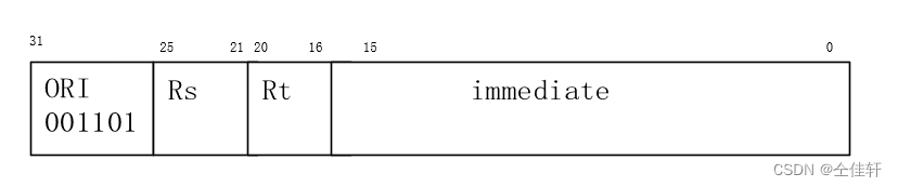
指令的用法为:ori rs,rt,immediate ,作用是将指令中的16位立即数immediate进行无符号扩展至32位,然后将索引位rs的通用寄存器的值进行逻辑的或运算,运算结果保存至索引为rt的通用寄存器中。
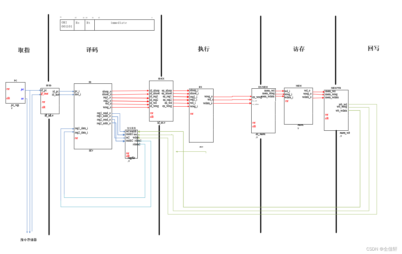
3.2 原始的OpenMips五级流水线结构
3.2.1 增加一些宏定义
// global define
`define RstEnable 1'b1
`define RstDisable 1'b0
`define WriteEnable 1'b1
`define WriteDisable 1'b0
`define ReadEnable 1'b1
`define ReadDisable 1'b0
`define AluOpBus    7:0 //the width of translation aluop_o
`define AluSelBus   2:0 //the width of translation alusel_o
`define InstVaild   1'b0 //vaild operator
`define InstInvaild 1'b1 //invaild operator
`define True_v      1'b1//meaning true
`define False_v     1'b0//meaning false
`define ChipDisable 1'b0
`define ChipEnable  1'b1
// something about operator
`define EXE_ORI 6'b001101     //the order of ori
`define EXE_NOP 6'b000000


//AluOp
`define EXE_OR_OP   8'b00100101
`define EXE_NOP_OP  8'b00000000

//AluSel
`define EXE_RES_LOGIC 3'b001
`define EXE_RES_NOP   3'b000
//instruction memory about rom
`define ZeroWord    32'h00000000
`define InstAddrBus 31:0  //address
`define InstBus     31:0 //Data
`define InstMemNum  131071 //rom fact size 128K
`define InstMemNumLog2 17     //the real width of rom


//************************ reg total define
`define RegAddrBus  4:0   //regfile addr width
`define RegBus      31:0  //regfile data width
`define RegWidth    32    //in common use reg width
`define DoubleRegwidth 64 // double reg width
`define DoubleRegBus  63:0 //double data width
`define RegNum        32 //the num of reg
`define RegNumLog2    5 //the num of common reg
`define NOPRegAddr    5'b00000
3.2.2 pc_reg.v
`timescale 1ns/1ns
`include "./src/defines.v"
module pc_reg (
    input wire    clk,
    input wire    rst,
    output reg[`InstAddrBus] pc,
    output reg ce
);
    always @(posedge clk) begin
        if(rst == `RstEnable) begin
            ce <= `ChipDisable;
        end
        else begin
            ce <= `ChipEnable;
        end
    end
    always @(posedge clk) begin
        if(ce == `ChipDisable) begin //disable. pc to 0
            pc <= `ZeroWord;
        end
        else begin
            pc <= pc + 4'h4;      //enable pc + 4
        end
    end
endmodule
当指令寄存器禁用的时候,PC的值保持为0,当指令寄存器使用的时候,PC值会在每时钟周期加四,表示下一一条指令的地址,因为一条指令是32位的,设计的处理器是可以按字节寻址,一条指令对应四个字节,所以PC+4表示指向下一条指令地址。
3.2.3 if/id.v
`timescale 1ns/1ns
`include "./src/defines.v"
module if_id(
    input wire clk,
    input wire rst,
    input wire[`InstAddrBus] if_pc,
    input wire[`InstBus]     if_inst,
    output reg[`InstAddrBus] id_pc,
    output reg[`InstBus]   id_inst
);
    always @(posedge clk) begin
        if(rst ==`RstEnable) begin
            id_pc <= `ZeroWord;
            id_inst <= `ZeroWord;
        end
        else begin
            id_pc <= if_pc;
            id_inst <= if_inst;
        end
    end
endmodule
这个地方书里解释的不是很清楚,其实是组合逻辑到时序逻辑的接口。将取指令阶段的结果在每个时钟上升阶段传递到译码阶段这个部分后文不再赘述,道理都是一样的。
3.2.4 regfile.v
`timescale 1ns/1ns
`include "./src/defines.v"
module regfile(
    input wire clk,
    input wire rst,

    // write
    input wire we,
    input wire[`RegAddrBus] waddr,
    input wire[`RegBus] wdata,

    // read one
    input wire  re1,
    input wire[`RegAddrBus] raddr1,
    output reg[`RegBus] rdata1,
    // read two
    input wire  re2,
    input wire[`RegAddrBus] raddr2,
    output reg[`RegBus] rdata2
);
//first define 32 nums of reg
reg[`RegBus] regs[0:`RegNum-1];
//second write
always @(posedge clk) begin
    if(rst == `RstDisable) begin
        if((we == `WriteEnable)&&(waddr != `RegNumLog2'h0)) begin
            regs[waddr] <= wdata;
        end
    end
end
//third read one
always @(*) begin
    if(rst == `RstEnable) begin
        rdata1 <= `ZeroWord;
    end else if (raddr1 == `RegNumLog2'h0) begin
        rdata1 <= `ZeroWord;
    end else if ((raddr1 == waddr)&&(we == `WriteEnable)&&(re1 == `ReadEnable)) begin
        rdata1 <= wdata;
    end else if (re1 == `ReadEnable) begin
        rdata1 <= regs[raddr1];
    end else begin
        rdata1 <= `ZeroWord;
    end
end
// read two
always @(*) begin
    if(rst == `RstEnable) begin
        rdata2 <= `ZeroWord;
    end else if (raddr2 == `RegNumLog2'h0) begin
        rdata2 <= `ZeroWord;
    end else if ((raddr2 == waddr)&&(we == `WriteEnable)&&(re2 == `ReadEnable)) begin
        rdata2 <= wdata;
    end else if (re2 == `ReadEnable) begin
        rdata2 <= regs[raddr2];
    end else begin
        rdata2 <= `ZeroWord;
    end
end
endmodule
regfile.v 可以分四段来进行理解
- 第一段定义了一个二维向量,元素个数为regnum,这在define.v有宏定义,表示32个通用寄存器。
- 第二段实现了寄存器写操作
- 第三段实现了寄存器的第一个读端口
- 第四段实现了寄存器第二个读端口
需要注意的是读端口是组合逻辑,当raddr1和raddr2和使能信号变换的时候,读出数据立即变换,可以保证译码阶段得到正确的地址值。而写操作是时序电路,写操作发生在时钟的上升沿。
3.2.5 id.v
`timescale 1ns/1ps
`include "./src/defines.v"
module id (
    input wire     rst,
    input wire[`InstAddrBus] pc_i,
    input wire[`InstBus] inst_i,
    //read the value of Regfile
    input wire[`RegBus] reg1_data_i,
    input wire[`RegBus] reg2_data_i,
    //output to Regfile
    output reg          reg1_read_o,
    output reg          reg2_read_o,
    output reg[`RegAddrBus] reg1_addr_o,
    output reg[`RegAddrBus] reg2_addr_o,
    //output to execute stage
    output reg[`AluOpBus] aluop_o,
    output reg[`AluSelBus] alusel_o,
    output reg[`RegBus]   reg1_o,
    output reg[`RegBus]   reg2_o,
    output reg[`RegAddrBus] wd_o,
    output reg wreg_o
);
//get order num and get function
//[26-31] is for ori ,you can judge if ori from it
wire[5:0] op = inst_i[31:26];
wire[4:0] op2 = inst_i[10:6];
wire[5:0] op3 = inst_i[5:0];
wire[4:0] op4 = inst_i[20:16];
// save need imediate num
reg[`RegBus] imm;
//judge vaildable
reg instvaild;
//stage one : decode
always @(*) begin
    if(rst ==`RstEnable) begin
        aluop_o <= `EXE_NOP_OP;
        alusel_o <= `EXE_RES_NOP;
        wd_o   <= `NOPRegAddr;
        wreg_o <= `WriteDisable;
        instvaild <= `InstVaild;
        reg1_read_o <= 1'b0;
        reg2_addr_o <= 1'b0;
        reg1_addr_o <= `NOPRegAddr;
        reg2_addr_o <= `NOPRegAddr;
        imm <= 32'h0;
    end else begin
         aluop_o <= `EXE_NOP_OP;
        alusel_o <= `EXE_RES_NOP;
        wd_o   <= inst_i[15:11];
        wreg_o <= `WriteDisable;
        instvaild <= `InstInvaild;
        reg1_read_o <= 1'b0;
        reg2_read_o <= 1'b0;
        reg1_addr_o <= inst_i[25:21];//default read from regfile pole one
        reg2_addr_o <= inst_i[20:16];//default read from regfile pole two
        imm <= `ZeroWord;
    case (op)
        `EXE_ORI:   begin
        //ori want to write in wanted write,so put wreg_o to writeable
        wreg_o <= `WriteEnable;
        //the subkind of compute is or
        aluop_o <= `EXE_OR_OP;
        //the kind of compute is  logic
        alusel_o <= `EXE_RES_LOGIC;
        //need Regfile one to read pole one
        reg1_read_o <= 1'b1;
        // not need Regfile two to read pole two
        reg2_read_o <= 1'b0;
        //execute immediate num
        imm <= {16'h0, inst_i[15:0]};
        //execute where you want to write in
        wd_o <= inst_i[20:16];
        // ori is Vaild;
        instvaild <= `InstVaild;
        end
        default: begin

        end
    endcase// case op
    end //if
end // always
//stage two : confirm source data one
always @(*) begin
    if(rst == `RstEnable) begin
        reg1_o <= `ZeroWord;
    end else if(reg1_read_o == 1'b1) begin
        reg1_o <= reg1_data_i; // Regfile Readone as input
    end else if (reg1_read_o == 1'b0) begin
        reg1_o <= imm; //imediate num
    end else begin
        reg1_read_o <=`ZeroWord;
    end
end
//stage three : confirm source data two
always @(*) begin
    if(rst == `RstEnable) begin
        reg2_o <= `ZeroWord;
    end else if(reg2_read_o == 1'b1) begin
        reg2_o <= reg1_data_i; // Regfile Readone as input
    end else if (reg2_read_o == 1'b0) begin
        reg2_o <= imm; //imediate num
    end else begin
        reg2_read_o <=`ZeroWord;
    end
end
endmodule
id模块都是组合电路,与regfile也有接口连接,可以分三个部分进行理解。
- 实现指令译码
- 给出参与操作的源数据1的值
- 给出参与操作源数据2的值
3.2.6 id/ex.v
`timescale 1ns/1ps
`include "./src/defines.v"
module id_ex (
    input wire   clk,
    input wire   rst,
    //message from decode
    input wire[`AluOpBus] id_aluop,
    input wire[`AluSelBus] id_alusel,
    input wire[`RegBus] id_reg1,
    input wire[`RegBus] id_reg2,
    input wire[`RegAddrBus] id_wd,
    input wire id_wreg,
    //output to execute stage
    output reg[`AluOpBus] ex_aluop,
    output reg[`AluSelBus] ex_alusel,
    output reg[`RegBus] ex_reg1,
    output reg[`RegBus] ex_reg2,
    output reg[`RegAddrBus] ex_wd,
    output reg ex_wreg
);
    always @(posedge clk) begin
        if(rst == `RstEnable) begin
            ex_aluop <= `EXE_NOP_OP;
            ex_alusel <= `EXE_RES_NOP;
            ex_reg1 <= `ZeroWord;
            ex_reg2 <= `ZeroWord;
            ex_wd <= `NOPRegAddr;
            ex_wreg <= `WriteDisable;
        end else begin
            ex_aluop <= id_aluop;
            ex_alusel <= id_alusel;
            ex_reg1 <= id_reg1;
            ex_reg2 <= id_reg2;
            ex_wd <= id_wd;
            ex_wreg <= id_wreg;
        end
    end

endmodule
3.2.7 ex.v
module ex (
    input wire rst,
    // from id to ex
    input wire[`AluOpBus] aluop_i,
    input wire[`AluSelBus] alusel_i,
    input wire[`RegBus] reg1_i,
    input wire[`RegBus] reg2_i,
    input wire[`RegAddrBus] wd_i,
    input wire wreg_i,
    //the result to output
    output reg[`RegAddrBus] wd_o,
    output reg wreg_o,
    output reg[`RegBus] wdata_o
);
//save the result of symbol compute
    reg[`RegBus] logicout;
//stage one: compute with aluop_i
    always @(*) begin
        if(rst == `RstEnable) begin
            logicout <= `ZeroWord;
        end else begin
            case(aluop_i)
                `EXE_OR_OP:begin
                    logicout <= reg1_i | reg2_i;
                end
                default: begin
                    logicout <= `ZeroWord;
                end
            endcase
        end//if
    end//always
//stage two: compute instead of alusel_i
    always @(*) begin
        wd_o <= wd_i;
        wreg_o <= wreg_i;
        case (alusel_i)
            `EXE_RES_LOGIC: begin
                wdata_o <= logicout;
            end
            default: begin
                wdata_o <= `ZeroWord;
            end
        endcase
    end

endmodule
ex 也均是组合电路,可以分两段来理解
- 第一段依据输入的子类型进行运算
- 第二段给出最终的结果向流水线下一级进行传递
3.2.8 ex/mem
`timescale 1ns/1ps
`include "./src/defines.v"
module ex_mem (
    input wire clk,
    input wire rst,
    //from exe
    input wire[`RegAddrBus] ex_wd,
    input wire ex_wreg,
    input wire[`RegBus] ex_wdata,
    //output to mem
    output reg[`RegAddrBus] mem_wd,
    output reg mem_wreg,
    output reg[`RegBus] mem_wdata
);
    always @(posedge clk) begin
            if(rst == `RstEnable) begin
                mem_wd <= `NOPRegAddr;
                mem_wreg <= `WriteDisable;
                mem_wdata <= `ZeroWord;
            end else begin
                mem_wd <= ex_wd;
                mem_wreg <= ex_wreg;
                mem_wdata <= ex_wdata;
            end//if
        end//always

endmodule
3.2.9 mem.v
`timescale 1ns/1ps
`include "./src/defines.v"
module mem (
    input wire rst,
    //come from execiton
    input wire[`RegAddrBus] wd_i,
    input wire wreg_i,
    input wire[`RegBus] wdata_i,
    //output result
    output reg[`RegAddrBus] wd_o,
    output reg wreg_o,
    output reg[`RegBus] wdata_o
);
always @(*) begin
    if(rst == `RstEnable) begin
        wd_o <= `NOPRegAddr;
        wreg_o <= `WriteEnable;
        wdata_o <= `ZeroWord;
    end else begin
        wd_o <= wd_i;
        wreg_o <= wreg_i;
        wdata_o <= wdata_i;
    end
end

endmodule
这里什么都没做,其实是没有加入内存的缘故,在后面会加以完善。
3.2.10 mem_wb.v
`timescale 1ns/1ps
`include "./src/defines.v"
module mem_wb (
    input wire clk,
    input wire rst,
    //come from execiton
    input wire[`RegAddrBus] mem_wd,
    input wire mem_wreg,
    input wire[`RegBus] mem_wdata,
    //output result
    output reg[`RegAddrBus] wb_wd,
    output reg wb_wreg,
    output reg[`RegBus] wb_wdata
);
always @(posedge clk) begin
    if(rst == `RstEnable) begin
        wb_wd <= `NOPRegAddr;
        wb_wreg <= `WriteEnable;
        wb_wdata <= `ZeroWord;
    end else begin
        wb_wd <= mem_wd;
        wb_wreg <= mem_wreg;
        wb_wdata <= mem_wdata;
    end
end

endmodule
将结果回写到寄存器组regfile.v中。
3.2.11 openmips顶层
`timescale 1ns/1ps
`include "./src/defines.v"
module openmips (
    input wire clk,
    input wire rst,
    input wire[`RegBus] rom_data_i,
    output wire[`RegBus] rom_addr_o,
    output wire rom_ce_o
);
//connect if/id to id
wire[`InstAddrBus] pc;
wire[`InstAddrBus] id_pc_i;
wire[`InstBus] id_inst_i;
//connect id to id/ex
wire[`AluOpBus] id_aluop_o;
wire[`AluSelBus] id_alusel_o;
wire[`RegBus] id_reg1_o;
wire[`RegBus] id_reg2_o;
wire id_wreg_o;
wire[`RegAddrBus] id_wd_o;
//id/ex to rx
wire[`AluOpBus] ex_aluop_i;
wire[`AluSelBus] ex_alusel_i;
wire[`RegBus] ex_reg1_i;
wire[`RegBus] ex_reg2_i;
wire ex_wreg_i;
wire[`RegAddrBus] ex_wd_i;
//ex to ex_mem
wire ex_wreg_o;
wire[`RegAddrBus] ex_wd_o;
wire[`RegBus] ex_wdata_o;
//ex_mem to mem
wire mem_wreg_i;
wire[`RegAddrBus] mem_wd_i;
wire[`RegBus] mem_wdata_i;
//_mem to mem/wb
wire mem_wreg_o;
wire[`RegAddrBus] mem_wd_o;
wire[`RegBus] mem_wdata_o;
//mem/wb to regfile
//ex_mem to mem
wire wb_wreg_i;
wire[`RegAddrBus] wb_wd_i;
wire[`RegBus] wb_wdata_i;
//id to regfile
wire reg1_read;
wire reg2_read;
wire[`RegBus] reg1_data;
wire[`RegBus] reg2_data;
wire[`RegAddrBus] reg1_addr;
wire[`RegAddrBus] reg2_addr;
//pc_reg
pc_reg pc_reg0(
    .clk(clk),
    .rst(rst),
    .pc(pc),
    .ce(rom_ce_o)
);
assign rom_addr_o = pc;
//if/id
if_id if_id0(
    .clk(clk),
    .rst(rst),
    .if_pc(pc),
    .if_inst(rom_data_i),
    .id_pc(id_pc_i),
    .id_inst(id_inst_i)
);
//id module
id id0(
    .rst(rst),
    .pc_i(id_pc_i),
    .inst_i(id_inst_i),
    //from regfile input
    .reg1_data_i(reg1_data),
    .reg2_data_i(reg2_data),
    // output to regfile
    .reg1_read_o(reg1_read),
    .reg2_read_o(reg2_read),
    .reg1_addr_o(reg1_addr),
    .reg2_addr_o(reg2_addr),
    //output to id/ex
    .aluop_o(id_aluop_o),
    .alusel_o(id_alusel_o),
    .reg1_o(id_reg1_o),
    .reg2_o(id_reg2_o),
    .wd_o(id_wd_o),
    .wreg_o(id_wreg_o)
    );
regfile regfile1(
    .clk(clk),
    .rst(rst),
    .we(wb_wreg_i),
    .waddr(wb_wd_i),
    .wdata(wb_wdata_i),
    .re1(reg1_read),
    .raddr1(reg1_addr),
    .rdata1(reg1_data),
    .re2(reg2_read),
    .raddr2(reg2_addr),
    .rdata2(reg2_data)
);
//id/ex
id_ex id_ex0(
    .clk(clk),
    .rst(rst),
    //message from id
    .id_aluop(id_aluop_o),
    .id_alusel(id_alusel_o),
    .id_reg1(id_reg1_o),
    .id_reg2(id_reg2_o),
    .id_wd(id_wd_o),
    .id_wreg(id_wreg_o),
    //message to ex
    .ex_aluop(ex_aluop_i),
    .ex_alusel(ex_alusel_i),
    .ex_reg1(ex_reg1_i),
    .ex_reg2(ex_reg2_i),
    .ex_wd(ex_wd_i),
    .ex_wreg(ex_wreg_i)
);
//ex model
ex ex0(
    .rst(rst),
    // message from if/ex
    .aluop_i(ex_aluop_i),
    .alusel_i(ex_alusel_i),
    .reg1_i(ex_reg1_i),
    .reg2_i(ex_reg2_i),
    .wd_i(ex_wd_i),
    .wreg_i(ex_wreg_i),
    // output to ex/mem
    .wd_o(ex_wd_o),
    .wreg_o(ex_wreg_o),
    .wdata_o(ex_wdata_o)
);
//ex/mem
ex_mem ex_mem0(
    .clk(clk),
    .rst(rst),
    //from ex
    .ex_wd(ex_wd_o),
    .ex_wreg(ex_wreg_o),
    .ex_wdata(ex_wdata_o),
     //to mem
    .mem_wd(mem_wd_i),
    .mem_wreg(mem_wreg_i),
    .mem_wdata(mem_wdata_i)
);
//mem
mem mem0(
    .rst(rst),
    //from ex/mem
    .wd_i(mem_wd_i),
    .wreg_i(mem_wreg_i),
    .wdata_i(mem_wdata_i),
     //to mem
    .wd_o(mem_wd_o),
    .wreg_o(mem_wreg_o),
    .wdata_o(mem_wdata_o)
);
//mem/wb
mem_wb mem_wb0(
    .clk(clk),
    .rst(rst),
    //from mem
    .mem_wd(mem_wd_o),
    .mem_wreg(mem_wreg_o),
    .mem_wdata(mem_wdata_o),
     //to mem
    .wb_wd(wb_wd_i),
    .wb_wreg(wb_wreg_i),
    .wb_wdata(wb_wdata_i)
);
endmodule
四.验证openmips功能
4.1 指令寄存器rom
`timescale 1ns/1ps
`include "./src/defines.v"
module inst_rom (
    input wire ce,
    input wire[`InstAddrBus] addr,
    output reg[`InstBus] inst
);
//define a array which size is InstMemNum,the width is InstBus
reg[`InstBus] inst_mem[0:`InstMemNum - 1];
// use file inst_rom.data to intialize the data reg
initial begin
    $readmemh("./src/inst_rom.data", inst_mem);
end
always @(*) begin
    if(ce == `ChipDisable) begin
        inst <= `ZeroWord;
    end else begin
        inst <= inst_mem[addr[`InstMemNumLog2+1: 2]];
    end
end

endmodule
4.2 最小spoc实现
`timescale 1ns/1ps
`include "./src/defines.v"
module openmips_min_sopc (
    input wire rst,
    input wire clk
);
//connect reg
wire[`InstAddrBus] inst_addr;
wire[`InstBus] inst;
wire rom_ce;
//example openmips
openmips openmips0(
    .clk(clk),
    .rst(rst),
    .rom_addr_o(inst_addr),
    .rom_data_i(inst),
    .rom_ce_o(rom_ce)
);
//example rom
inst_rom inst_rom0(
    .ce(rom_ce),
    .addr(inst_addr),
    .inst(inst)
);

endmodule
4.3 搭建testbench
`timescale 1ns/1ps
`include "./src/defines.v"
module openmips_min_sopc_tb();

reg CLOCK_50;
reg rst;
//every 10 ns reverse clock
 initial begin
    CLOCK_50 = 1'b0;
    forever #10 CLOCK_50 = ~CLOCK_50;
 end

 initial begin
    rst =`RstEnable;
    #195 rst = `RstDisable;
    #1000  $finish;
 end
 openmips_min_sopc  openmips_min_sopc0(
    .clk(CLOCK_50),
    .rst(rst)
 );
 initial begin
	$fsdbDumpfile("tb.fsdb");
	$fsdbDumpvars("+all");
end
 endmodule
4.4 生成机器码 .data文件
编译工具链:
链接:https://pan.baidu.com/s/1tA-FIUkCrGYNC9AwhCniNA
提取码:1999
将上述文件导入到linux环境下
cd $下载路径$
tar vfxj mips-sde-elf-1686-pc-linux-gnu.tar.tar
export PATH="$PATH:/$下载路径$/mips-4.3/bin"
在虚拟机中新建一个文件inst_rom.S
	.org 0x0
.global _start
   .set noat
_start:
   ori $1,$0,0x1100        # $1 = $0 | 0x1100 = 0x1100
   ori $2,$0,0x0020        # $2 = $0 | 0x0020 = 0x0020
   ori $3,$0,0xff00        # $3 = $0 | 0xff00 = 0xff00
   ori $4,$0,0xffff        # $4 = $0 | 0xffff = 0xffff
编写makefile
ifndef CROSS_COMPILE
CROSS_COMPILE = mips-sde-elf-
endif
CC = $(CROSS_COMPILE)as
LD = $(CROSS_COMPILE)ld
OBJCOPY = $(CROSS_COMPILE)objcopy
OBJDUMP = $(CROSS_COMPILE)objdump

OBJECTS = inst_rom.o

export	CROSS_COMPILE

# ********************
# Rules of Compilation
# ********************

all: inst_rom.om inst_rom.bin inst_rom.asm inst_rom.data

%.o: %.S
	$(CC) -mips32 $< -o $@
inst_rom.om: ram.ld $(OBJECTS)
	$(LD) -T ram.ld $(OBJECTS) -o $@
inst_rom.bin: inst_rom.om
	$(OBJCOPY) -O binary $<  $@
inst_rom.asm: inst_rom.om
	$(OBJDUMP) -D $< > $@
inst_rom.data: inst_rom.bin
	./Bin2Mem.exe -f $< -o $@
clean:
	rm -f *.o *.om *.bin *.data *.mif *.asm
将编写的Makefile和Bin2Mem.exe,ramld放到源代码同一目录下,执行make all。即可生成inst_rom.data文件。
4.5 在verdi中验证功能
make compile
make verdi

五.总结
- 这篇博客通过实现指令ori,搭建了一个原始的五级流水线结构,这是openmips最核心的内容。
- 使用汇编语言生成机器码,在verdi+vcs环境下进行了功能验证。


 568
568

 被折叠的 条评论
为什么被折叠?
被折叠的 条评论
为什么被折叠?
 到【灌水乐园】发言


