


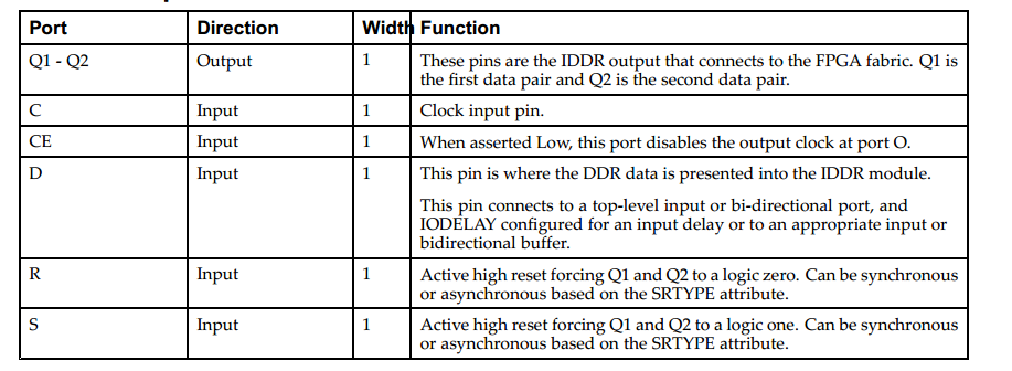
Port Descriptions
方式一:
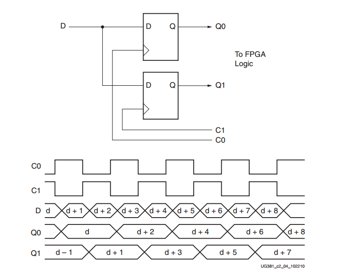
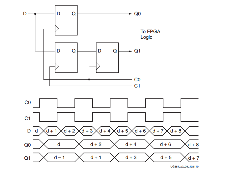
At some point in a design, both signals must be brought into the same clock domain,typically C0. This can be difficult at high frequencies because the available time is only one half of a clock cycle assuming a 50% duty cycle. The IDDR2 contains dedicated paths to allow this clock domain transition to occur inside the ILOGIC2 block.
方式二:
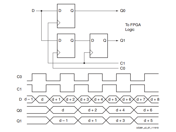
When DDR_ALIGNMENT = C0 (or C1), the signal Q1 (Q0) is re-registered to C0 (C1), and is only then fed to the interconnect CLB logic keeping the outputs in the same clock domain. Figure illustrates how the interconnecting logic uses only the clock C0 to
forward the received data.
方式三:
// IDDR2: Input Double Data Rate Input Register with Set, Reset
// and Clock Enable.

**// Spartan-3E/3A/6**

// Xilinx HDL Libraries Guide, version 11.2
IDDR2 #(
.DDR_ALIGNMENT("NONE"), // Sets output alignment to "NONE", "C0" or "C1"
.INIT_Q0(1’b0), // Sets initial state of the Q0 output to 1’b0 or 1’b1
.INIT_Q1(1’b0), // Sets initial state of the Q1 output to 1’b0 or 1’b1
.SRTYPE("SYNC") // Specifies "SYNC" or "ASYNC" set/reset
) IDDR2_inst (
.Q0(Q0), // 1-bit output captured with C0 clock
.Q1(Q1), // 1-bit output captured with C1 clock
.C0(C0), // 1-bit clock input
.C1(C1), // 1-bit clock input
.CE(CE), // 1-bit clock enable input
.D(D), // 1-bit DDR data input
.R(R), // 1-bit reset input
.S(S) // 1-bit set input
);

-------------------------------------------------

// IDDR: Input Double Data Rate Input Register with Set, Reset
// and Clock Enable.

**// 7 Series**

// Xilinx HDL Libraries Guide, version 14.2
IDDR #(
.DDR_CLK_EDGE("OPPOSITE_EDGE"), // "OPPOSITE_EDGE", "SAME_EDGE"
// or "SAME_EDGE_PIPELINED"
.INIT_Q1(1'b0), // Initial value of Q1: 1'b0 or 1'b1
.INIT_Q2(1'b0), // Initial value of Q2: 1'b0 or 1'b1
.SRTYPE("SYNC") // Set/Reset type: "SYNC" or "ASYNC"
) IDDR_inst (
.Q1(Q1), // 1-bit output for positive edge of clock
.Q2(Q2), // 1-bit output for negative edge of clock
.C(C), // 1-bit clock input
.CE(CE), // 1-bit clock enable input
.D(D), // 1-bit DDR data input
.R(R), // 1-bit reset
.S(S) // 1-bit set
);
使用例程参考:
module RGMII_rx_ctrl (
                    //from phy
                    input wire rx_clk,   //125M
                    input wire rst_n,
                    input wire rx_dv,//千兆网同步有效信号,双沿采样  上升沿=dv 下降沿=deer
                    input wire [3:0]rx_data,

                    //to mac //物理层
                    output reg rx_en,
                    output reg [7:0]o_data//单沿采样数据
                );


    wire tmp_dv;
    wire tmp_err;//rxdv,rxerr
    wire [7:0]tmp_data;

    //例化5次,一次使能,4次数据
    // IDDR2: Input Double Data Rate Input Register with Set, Reset
    // and Clock Enable.
    // Spartan-3E/3A/6
    // Xilinx HDL Libraries Guide, version 11.2
    IDDR2 #(
            .DDR_ALIGNMENT("NONE"), // Sets output alignment to "NONE", "C0" or "C1"
            .INIT_Q0(1'b0), // Sets initial state of the Q0 output to 1’b0 or 1’b1
            .INIT_Q1(1'b0), // Sets initial state of the Q1 output to 1’b0 or 1’b1
            .SRTYPE("SYNC") // Specifies "SYNC" or "ASYNC" set/reset
            )
    IDDR2_inst (
            .Q0(tmp_dv), // 1-bit output captured with C0 clock
            .Q1(tmp_err), // 1-bit output captured with C1 clock
            .C0(rx_clk), // 1-bit clock input
            .C1(~rx_clk), // 1-bit clock input
            .CE(1'b1), // 1-bit clock enable input
            .D(rx_dv), // 1-bit DDR data input
            .R(1'b0), // 1-bit reset input
            .S(~rst_n) // 1-bit set input
            );
    // End of IDDR2_inst instantiation

    genvar i;
    generate
        for(i=0;i<4;i=i+1)begin
            IDDR2 #(
            .DDR_ALIGNMENT("NONE"), // Sets output alignment to "NONE", "C0" or "C1"
            .INIT_Q0(1'b0), // Sets initial state of the Q0 output to 1’b0 or 1’b1
            .INIT_Q1(1'b0), // Sets initial state of the Q1 output to 1’b0 or 1’b1
            .SRTYPE("SYNC") // Specifies "SYNC" or "ASYNC" set/reset
            )
            IDDR2_inst_r (
            .Q0(tmp_data[i]), // 1-bit output captured with C0 clock
            .Q1(tmp_data[i+4]), // 1-bit output captured with C1 clock
            .C0(rx_clk), // 1-bit clock input
            .C1(~rx_clk), // 1-bit clock input
            .CE(1'b1), // 1-bit clock enable input
            .D(rx_data[i]), // 1-bit DDR data input
            .R(1'b0), // 1-bit reset input
            .S(~rst_n) // 1-bit set input
            );
        end
    endgenerate

    always @(posedge rx_clk)
    if(!rst_n)
        o_data <= 'd0;
    else
        o_data <= tmp_data;

    always @(posedge rx_clk)
    if(!rst_n)
        rx_en <= 'd0;
    else
        rx_en <= tmp_dv;

endmodule


 1038
1038

 被折叠的 条评论
为什么被折叠?
被折叠的 条评论
为什么被折叠?
 到【灌水乐园】发言


