


About CACHE 1. cache introduction A cache is a small, fast array of memory placed between the processor core and main memory that stores portions of recently referenced main memory. The processor uses cache-memory instead of main-memory whenever possible to increase system performance. The goal of a cache is to reduce the memory access bottleneck imposed on the processor core by slow memory. 2. write buffer introduction Write buffer: a very small first-in-first-out (FIFO) memory placed between the processor core and main memory. The purpose of a write buffer is to free the processor core and cache memory from the slow write time associated with writing to main memory. 3. the role of the cache The basic unit of storage in a cache is the cache line. A cache line is said to be valid when it contains cached data or instructions, and invalid when it does not. All cache lines in a cache are invalidated on reset. A cache line becomes valid when data or instructions are loaded into it from memory. When a cache line is valid, it contains up-to-date values for a block of consecutive main memory locations. The length of a cache line is always a power of two, and is typically in the range of 16 to 64 bytes. If the cache line length is 2L bytes, the block of main memory locations is always 2L-byte aligned. Because of this alignment requirement, virtual address bits[31:L] are identical for all bytes in a cache line 4. the location of the cache The cache can choose different location: physical & logical caches. 5. the types of cache there are two types cache: Write Through : when reading, read from the cache; when writing, write to the cache first and write to the main memory at the same time. Write Back: when reading, read from the cache; when writing, just write to the cache, and until the cache expire or explicit implement flush operation, the data will be written to the memory. 6. the operations of cache Invalidate : enable the cache, so it will be “Miss” cache when to read next time and to read from the memory instead. Flush : the data in the cache will be written to the memory. Some types of cpu use CACHE based on the physical memory address, and the others use CACHE based on Virtual address. Based on physical address: do not need to invalidate cache when process switching, but the performance is a little lower because the MMU has to convert the virtual address to physical address so that to decide whether the cache hitting. Based on virtual address: got high performance, but it need to invalidated the cache when process switching. Most of the cpu use the method based on virtual address. 7. the basic structure of the cache Cache is always realized by the associative memory. Every storage block in the associative memory has extra information, called “Tag”. When accessing the associative memory, the address will be compared with each Tag and the storage block which has the same tag will be accessed. Dcache: ARM cache structure is made up of cache memory and write buffer. Usually CACHEABILITY and BUFFERABILITY can be configured. One storage area can be configured as: NCNB, CNB, NCB, CB. Dcache uses virtual address, the size is 16KB, divided into 512 entry, 8 words for each entry,two dirty bits for each entry, a tag and a valid bit for each entry. On reset or power on, DCache is disabled. Set Ccr bit to enable DCache. Dcache can be used after MMU is enabled.
ICache: The ICache is organized as eight segments, each containing 64 lines, and each line containing eight words. The position of the line within the segment is a number from 0 to 63. This is called the index. A line in the cache can be uniquely identified by its segment and index. The index is independent of the MVA. The segment is selected by bits [7:5] of the MVA. Bits [4:2] of the MVA specify the word within a cache line that is accessed. For halfword operations, bit [1] of the MVA specifies the halfword that is accessed within the word. For byte operations, bits [1:0] specify the byte within the word that is accessed. Bits [31:8] of the MVA of each cache line are called the TAG. The MVA TAG is store in the cache, along with the 8-words of data, when the line is loaded by a linefill. Cache lookups compare bits [31:8] of the MVA of the access with the stored TAG to determine whether the access is a hit or miss. The cache is therefore said to be virtually addressed.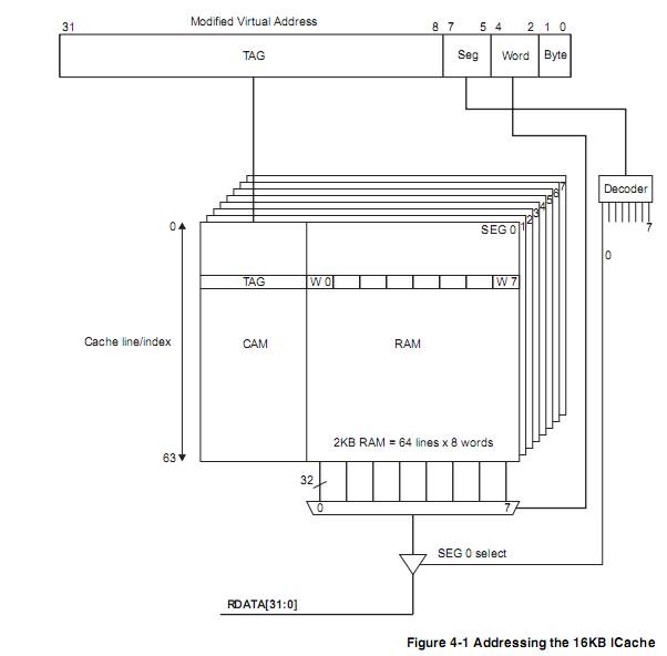
On reset, the ICache entries are all invalidated and the ICache is disabled. You can enable the ICache by writing 1 to the Icr bit, and disable it by writing 0 to the Icr bit. When the ICache is disabled, the cache contents are ignored and all instruction fetches appear on the AMBA ASB interface as separate nonsequential accesses. The ICache is usually used with the MMU enabled. In this case the Ctt in the relevant MMU translation table descriptor indicates whether an area of memory is cachable. If the cache is disabled after having been enabled, all cache contents are ignored. All instruction fetches appear on the AMBA ASB interface as separate nonsequential accesses and the cache is not updated. If the cache is subsequently re-enabled its contents are unchanged. If the contents are no longer coherent with main memory, you must invalidate the ICache before you re-enable it. 8. Situations that necessitate cache cleaning and invalidating include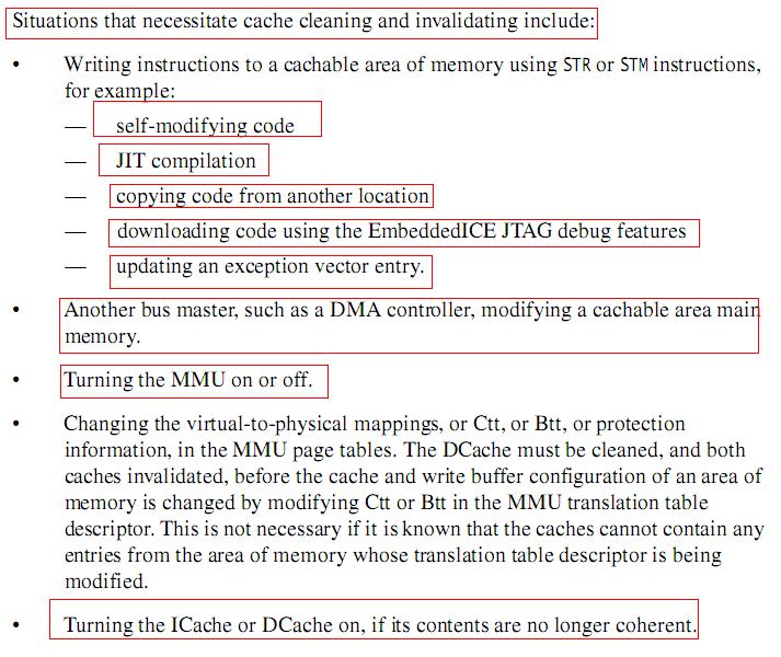


 714
714

 被折叠的 条评论
为什么被折叠?
被折叠的 条评论
为什么被折叠?
 到【灌水乐园】发言


