


FPGA学习
Quatus软件Verilog调用同步FIFO ip核步骤
前言
FIFO(First In First Out,即先入先出),是一种数据缓冲器,用来实现数据先入先出的读写方式。与 ROM 或 RAM 的按地址读写方式不同,FIFO 的读写遵循“先进先出”的原则,即数据按顺序写入 FIFO,先被写入的数据同样在读取的时候先被读出,所以 FIFO存储器没有地址线。FIFO有一个写端口和一个读端口外部无需使用者控制地址,使用方便。
一、同步FIFO工作流程
FIFO 存储器主要是作为缓存,应用在同步时钟系统和异步时钟系统中,在很多的设计中都会使用,后面实例中如:多比特数据做跨时钟域的转换、前后带宽不同步等都用到了FIFO。FIFO 根据读写时钟是否相同,分为 SCFIFO(同步 FIFO)和 DCFIFO(异步 FIFO),SCFIFO 的读写为同一时钟,应用在同步时钟系统中;DCFIFO 的读写时钟不同,应用在异步时钟系统中。
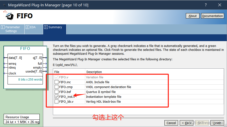
二、配置FIFOip核工作流程
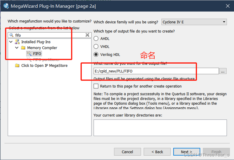
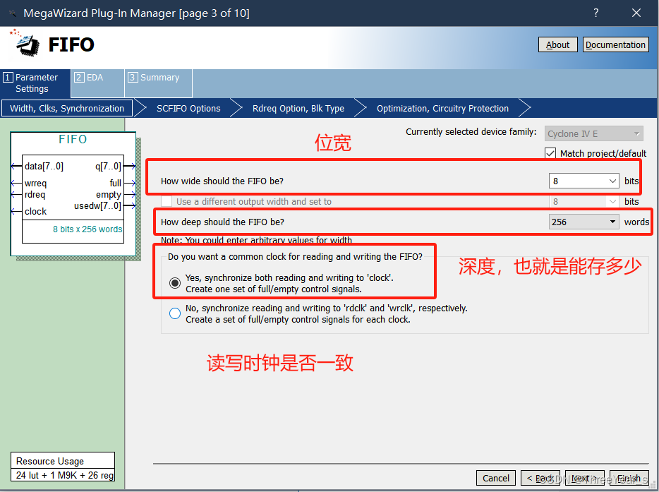
中间没有截图的都是默认next
调用
module PLL
(
input wire sys_clk , //系统时钟50MHz
input wire sys_rst_n,
input wire [7:0] pi_data , //输入顶层模块的数据
input wire pi_flag , //输入数据有效标志信号//也作为FIFO的写请求信号
input wire rdreq , //FIFO读请求信号
output wire [7:0] po_data , //FIFO读出的数据
output wire empty , //FIFO空标志信号,高有效
output wire full , //FIFO满标志信号,高有效
output wire [7:0] usedw, //FIFO中存在的数据个数
output wire clk_mul_2 , //系统时钟经过2倍频后的时钟
output wire clk_div_2 , //系统时钟经过2分频后的时钟
output wire clk_phase_90 , //系统时钟经过相移90°后的时钟
output wire clk_ducle_20 , //系统时钟变为占空比为20%的时钟
output wire locked //检测锁相环是否已经锁定,
//只有该信号为高时输出的时钟才是稳定的
);
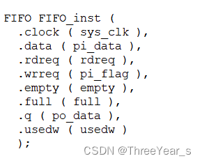
//\* Instantiation \//
FIFO FIFO_inst (
.clock ( sys_clk ),
.data ( pi_data ),
.rdreq ( rdreq ),
.wrreq ( pi_flag ),
.empty ( empty ),
.full ( full ),
.q ( po_data ),
.usedw ( usedw )
);
//------------------------pll_ip_inst------------------------
PLL_20 PLL_20_inst (
.areset ( sys_rst_n ),
.inclk0 ( sys_clk ),
.c0 ( clk_mul_2 ),
.c1 ( clk_div_2 ),
.c2 ( clk_phase_90 ),
.c3 ( clk_ducle_20 ),
.locked ( locked )
);
endmodule
tb文件:
// Copyright (C) 1991-2013 Altera Corporation
// Your use of Altera Corporation's design tools, logic functions
// and other software and tools, and its AMPP partner logic
// functions, and any output files from any of the foregoing
// (including device programming or simulation files), and any
// associated documentation or information are expressly subject
// to the terms and conditions of the Altera Program License
// Subscription Agreement, Altera MegaCore Function License
// Agreement, or other applicable license agreement, including,
// without limitation, that your use is for the sole purpose of
// programming logic devices manufactured by Altera and sold by
// Altera or its authorized distributors.  Please refer to the
// applicable agreement for further details.

// *****************************************************************************
// This file contains a Verilog test bench template that is freely editable to
// suit user's needs .Comments are provided in each section to help the user
// fill out necessary details.
// *****************************************************************************
// Generated on "06/01/2024 14:50:33"

// Verilog Test Bench template for design : PLL
//
// Simulation tool : ModelSim-Altera (Verilog)
//

`timescale 1 ns/ 1 ps
module PLL_vlg_tst();
// constants
// general purpose registers
// test vector input registers
reg sys_rst_n;
reg sys_clk;
reg [7:0] pi_data ;
reg pi_flag ;
reg rdreq ;

// wires
wire clk_div_2;
wire clk_ducle_20;
wire clk_mul_2;
wire clk_phase_90;
wire locked;
wire [7:0] po_data ;
 wire empty ;
 wire full ;
 wire [7:0] usedw ;

// assign statements (if any)
PLL i1 (
// port map - connection between master ports and signals/registers
	.clk_div_2(clk_div_2),
	.clk_ducle_20(clk_ducle_20),
	.clk_mul_2(clk_mul_2),
	.clk_phase_90(clk_phase_90),
	.locked(locked),
	.sys_rst_n(sys_rst_n),
	.pi_data (pi_data ), //input [7:0] pi_data
 .pi_flag (pi_flag ), //input pi_flag
 .rdreq (rdreq ), //input rdreq

 .po_data (po_data ), //output [7:0] po_data
 .empty (empty ), //output empty
 .full (full ), //output full
 .usedw (usedw ), //output [7:0] usedw
	.sys_clk(sys_clk)
);
initial
begin
sys_clk <=  1'b1;
sys_rst_n   <= 1'b0;
#200
sys_rst_n   <= 1'b1;

end
always  #10 sys_clk=~sys_clk;
     reg [1:0] cnt_baud ;
//cnt_baud:计数从0到3的计数器,用于产生输入数据间的间隔
 always@(posedge sys_clk or negedge sys_rst_n)
 if(sys_rst_n == 1'b0)
 cnt_baud <= 2'b0;
 else if(&cnt_baud == 1'b1)
 cnt_baud <= 2'b0;
 else
 cnt_baud <= cnt_baud + 1'b1;

 //pi_flag:输入数据有效标志信号,也作为FIFO的写请求信号
 always@(posedge sys_clk or negedge sys_rst_n)
 if(sys_rst_n == 1'b0)
 pi_flag <= 1'b0;
 //每4个时钟周期且没有读请求时产生一个数据有效标志信号
 else if((cnt_baud == 2'd0) && (rdreq == 1'b0))
 pi_flag <= 1'b1;
 else
 pi_flag <= 1'b0;

 //pi_data:输入顶层模块的数据,要写入到FIFO中的数据
 always@(posedge sys_clk or negedge sys_rst_n)
 if(sys_rst_n == 1'b0)
 pi_data <= 8'b0;
 //pi_data的值为0~255依次循环
 else if((pi_data == 8'd255) && (pi_flag == 1'b1))
 pi_data <= 8'b0;
 else if(pi_flag == 1'b1) //每当pi_flag有效时产生一个数据
 pi_data <= pi_data + 1'b1;

 //rdreq:FIFO读请求信号
 always@(posedge sys_clk or negedge sys_rst_n)
 if(sys_rst_n == 1'b0)
 rdreq <= 1'b0;
 else if(full == 1'b1) //当FIFO中的数据存满时,开始读取FIFO中的数据
 rdreq <= 1'b1;
 else if(empty == 1'b1) //当FIFO中的数据被读空时停止读取FIFO中的数据
 rdreq <= 1'b0;
endmodule
总结
FIFO就是如果两个人同频,那么你们永远都不会走散,我的爱意先进先出,但是存满就会表达爱意哦~


 1505
1505


 被折叠的 条评论
为什么被折叠?
被折叠的 条评论
为什么被折叠?
 到【灌水乐园】发言


