


前言
1、mpc5748G开发板学习笔记(一:点灯)记录了开发环境配置和GPIO的IO操作,并顺利的点亮了一排LED灯
本文将使用MPC5748G自带的电位器输入端口PB[4],测试一下ADC模块。
1 外围设备
PB[4]引脚的电路图如图下所示:

可以看到电位器RV1阻值为5K欧姆,左侧引脚3接3.3V高电平,右侧1接地,中间引脚2通过一个0欧的R131电阻接PB[4]端口。所以该电位器起到了分压的作用,当电位器2号引脚滑动到最左侧时,PB[4]电压为3.3V,反之为0V。
所以PB[4]引脚模拟量的电压接收范围为 0 ~ 3.3V,使用的ADC通道为ADC1 P[0],手册中得知ADC1的精度为12bit,所以PB[4]输出数字量的范围为:0 ~ 4095 ,对应0 ~ 3.3V的电压。
2 编程思路
SDK给的ADC模块例程使用了一个LED灯PJ[4],当模拟量输入低于1.6V灯灭,高于1.6V灯亮。
想要将模拟量的输入更形象的表示出来,可以借用上一篇文章的8个LED显示,将3.3V电压切分为8段,每一段点亮一个LED灯,可以更加直观的看到模拟信号的变化。
3 SDK生成代码
(1)新建工程
- 点击File -> New -> S32DS Application Project

- 给项目命名并选择MPC5748G,点击Next。
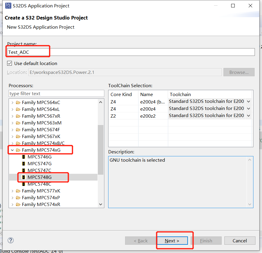
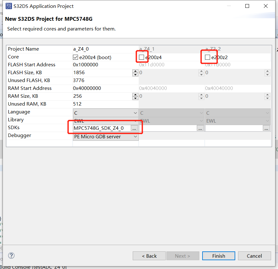
- 只用一个Z4核就可以了,反选其他两个核,选择SDK。
(2)配置adConv1:adc_sar模块
- 双击pin_mux -> 点击Components Library -> 双击adc_sar。
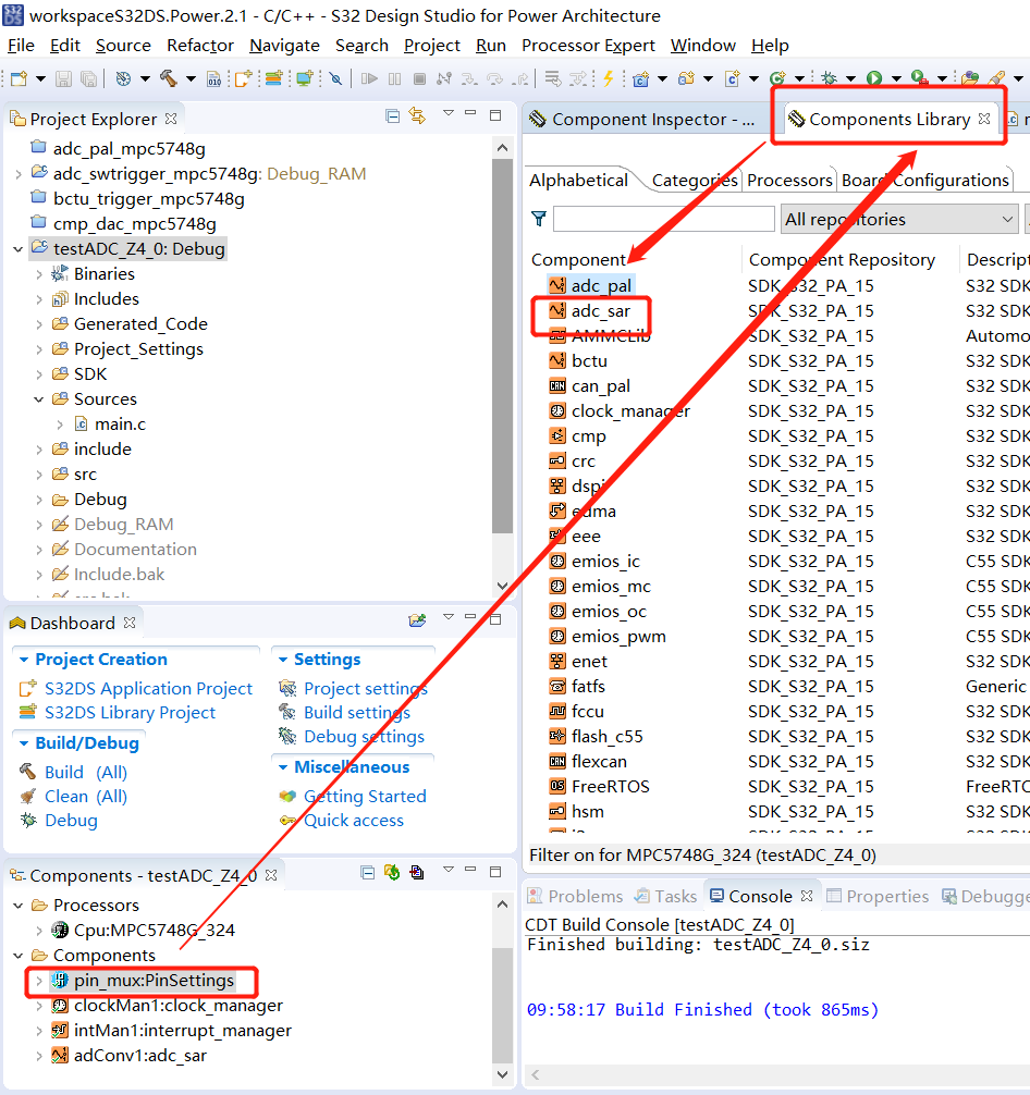
- 双击adConv1:adc_sar ,反选 Chain Configurations。

- 将Sample duration 0 和1 2数值改为20。

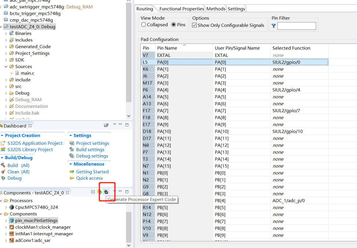
(3)配置pin_mux
- 双击pin_mux模块,点击ADC栏,将ADC1中的precision channal 0选中
PB[4]

- 选中pins,把所有的LED模块选为gpio out,具体参考上一篇文章。

- 配置完成后点击生成代码。
4 主函数编写
/* ###################################################################
** Filename : main.c
** Project : testADC
** Processor : MPC5748G_176
** Version : Driver 01.00
** Compiler : GNU C Compiler
** Date/Time : 2017-03-14, 14:08, # CodeGen: 1
** Abstract :
** Settings :
** Contents :
**
** ###################################################################*/
/*!
** @file main.c
** @version 01.00
** @brief
** Main module.
** This module contains user's application code.
*/
/*!
** @addtogroup main_module main module documentation
** @{
*/
/* MODULE main */
/* Including needed modules to compile this module/procedure */
#include "Cpu.h"
#include "clockMan1.h"
#include "adConv1.h"
#include "pin_mux.h"
volatile int exit_code = 0;
/* User includes (#include below this line is not maintained by Processor Expert) */
#include <stdint.h>
#include <stdbool.h>
/* This example is setup to work by default with DEVKIT. To use it with other boards
please comment the following line
*/
#define DEVKIT
#ifdef DEVKIT
#define PORT0 PTA
#define LED0 10
#define PORT1 PTA
#define LED1 7
#define PORT2 PTH
#define LED2 13
#define PORT3 PTC
#define LED3 4
#define PORT4 PTH
#define LED4 5
#define PORT5 PTJ
#define LED5 4U
#define PORT6 PTA
#define LED6 0
#define PORT7 PTA
#define LED7 4
#define ADC_CHAN_NUM (9u) /* ADC1_P[0] corresponding to PB[4] */
uint16_t result; /* 读取PB[4]的结果 */
#define ADC_THRESHOLD (512u) /* should be around 3.3V/8 = 0.4125V for 12-bit resolution,
4096/8 = 512 也就是 3.3V/8 的数字量 */
/*!
\brief The main function for the project.
\details The startup initialization sequence is the following:
* - startup asm routine
* - main()
*/
int main(void)
{
/* Write your local variable definition here */
/*** Processor Expert internal initialization. DON'T REMOVE THIS CODE!!! ***/
#ifdef PEX_RTOS_INIT
PEX_RTOS_INIT(); /* Initialization of the selected RTOS. Macro is defined by the RTOS component. */
#endif
/*** End of Processor Expert internal initialization. ***/
/* Initialize and configure pins */
PINS_DRV_Init(NUM_OF_CONFIGURED_PINS, g_pin_mux_InitConfigArr);
/* Initialize clocks */
CLOCK_SYS_Init(g_clockManConfigsArr, CLOCK_MANAGER_CONFIG_CNT,
g_clockManCallbacksArr, CLOCK_MANAGER_CALLBACK_CNT);
CLOCK_SYS_UpdateConfiguration(0U, CLOCK_MANAGER_POLICY_AGREEMENT);
/* Initialize ADC */
ADC_DRV_Reset(INST_ADCONV1); //复位
ADC_DRV_DoCalibration(INST_ADCONV1); //校准
ADC_DRV_ConfigConverter(INST_ADCONV1,&adConv1_ConvCfg0); //配置
ADC_DRV_EnableChannel(INST_ADCONV1, ADC_CONV_CHAIN_NORMAL, ADC_CHAN_NUM); //使能
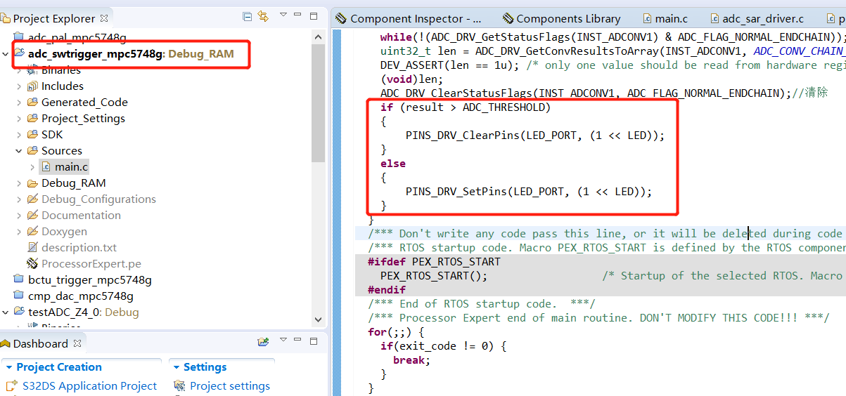
/* Start a loop to read converted values and blink an LED */
while(1)
{
ADC_DRV_StartConversion(INST_ADCONV1, ADC_CONV_CHAIN_NORMAL); //启动
while(!(ADC_DRV_GetStatusFlags(INST_ADCONV1) & ADC_FLAG_NORMAL_ENDCHAIN)); //等待状态标志
uint32_t len = ADC_DRV_GetConvResultsToArray(INST_ADCONV1, ADC_CONV_CHAIN_NORMAL, &result, 1u); //获取转换结果
DEV_ASSERT(len == 1u); /* only one value should be read from hardware registers */
(void)len;
ADC_DRV_ClearStatusFlags(INST_ADCONV1, ADC_FLAG_NORMAL_ENDCHAIN);//清除
uint8_t ledValue = 0x00;
if(result < (1 * ADC_THRESHOLD))
{
ledValue = 0x01; //点亮LED0 0b0000 0001
}
else if(((1 * ADC_THRESHOLD) <=result) && (result < (2 * ADC_THRESHOLD)))
{
ledValue = 0x02; //点亮LED1
}
else if(((2 * ADC_THRESHOLD) <=result) && (result < (3 * ADC_THRESHOLD)))
{
ledValue = 0x04; //点亮LED2
}
else if(((3 * ADC_THRESHOLD) <=result) && (result < (4 * ADC_THRESHOLD)))
{
ledValue = 0x08; //点亮LED3
}
else if(((4 * ADC_THRESHOLD) <=result) && (result < (5 * ADC_THRESHOLD)))
{
ledValue = 0x10; //点亮LED4
}
else if(((5 * ADC_THRESHOLD) <=result) && (result < (6 * ADC_THRESHOLD)))
{
ledValue = 0x20; //点亮LED5
}
else if(((6 * ADC_THRESHOLD) <=result) && (result < (7 * ADC_THRESHOLD)))
{
ledValue = 0x40; //点亮LED6
}
else if(((7 * ADC_THRESHOLD) <=result) && (result < (8 * ADC_THRESHOLD)))
{
ledValue = 0x80; //点亮LED7 0b1000 0000
}
else
{
}
PINS_DRV_WritePin(PORT0, LED0, (ledValue & 0x01) ? 0 : 1);
PINS_DRV_WritePin(PORT1, LED1, (ledValue & 0x02) ? 0 : 1);
PINS_DRV_WritePin(PORT2, LED2, (ledValue & 0x04) ? 0 : 1);
PINS_DRV_WritePin(PORT3, LED3, (ledValue & 0x08) ? 0 : 1);
PINS_DRV_WritePin(PORT4, LED4, (ledValue & 0x10) ? 0 : 1);
PINS_DRV_WritePin(PORT5, LED5, (ledValue & 0x20) ? 0 : 1);
PINS_DRV_WritePin(PORT6, LED6, (ledValue & 0x40) ? 0 : 1);
PINS_DRV_WritePin(PORT7, LED7, (ledValue & 0x80) ? 0 : 1);
}
/*** Don't write any code pass this line, or it will be deleted during code generation. ***/
/*** RTOS startup code. Macro PEX_RTOS_START is defined by the RTOS component. DON'T MODIFY THIS CODE!!! ***/
#ifdef PEX_RTOS_START
PEX_RTOS_START(); /* Startup of the selected RTOS. Macro is defined by the RTOS component. */
#endif
/*** End of RTOS startup code. ***/
/*** Processor Expert end of main routine. DON'T MODIFY THIS CODE!!! ***/
for(;;) {
if(exit_code != 0) {
break;
}
}
return exit_code;
/*** Processor Expert end of main routine. DON'T WRITE CODE BELOW!!! ***/
} /*** End of main routine. DO NOT MODIFY THIS TEXT!!! ***/
/* END main */
/*!
** @}
*/
/*
**
*/
具体每一行代码的功能已经注释进去了,但是这一句代码困扰了我很久,最后还是问了导师:
#define ADC_CHAN_NUM (9u) /* ADC1_P[0] corresponding to PB[4] */
问题:这个宏定义里的9到底是在哪里出来的?
回答:可以在MPC5748G的用户手册752页找到。
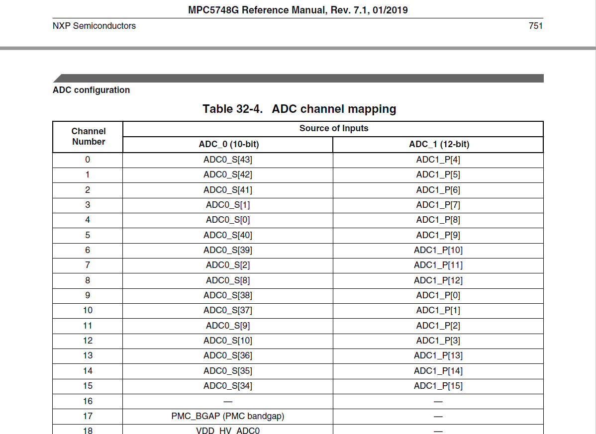
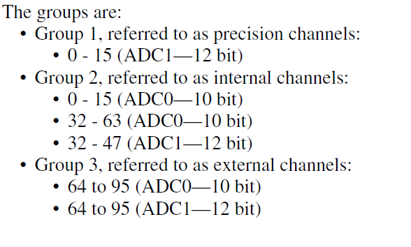
- 因为5748G的ADC有两个,通道又各有96路,分为3组如图所示,所以查看具体的通道编号需要查表,可以看到ADC1_P[0]的Channel Number确实就是9。
5 代码烧写
烧写过程参阅mpc5748G开发板学习笔记(一:点灯)的第6步。
烧录到RAM和Flash都可以,RAM中的数据断电后会丢失,但是烧写速度更快,Flash里的程序可以一直保存下去,每次reset都会自动运行。
小锤子可以选择编译方式:
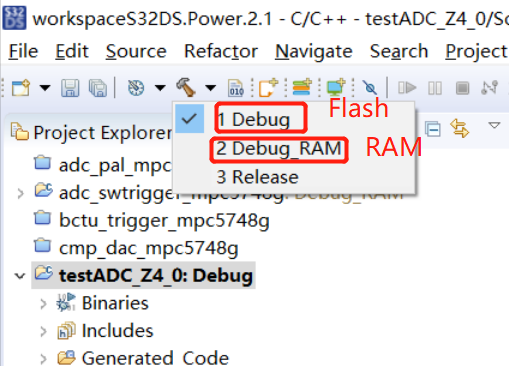
Debug选择烧到RAM还是Flash里,这里选择的是Flash:

6 程序运行
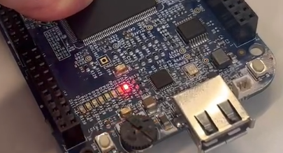
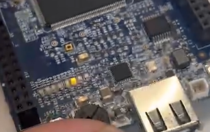
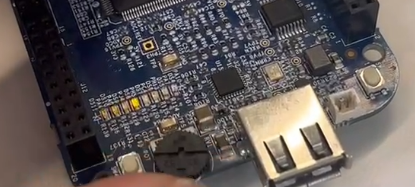
可以看到转动电位器会导致LED发生变化。
代码已上传github:
https://github.com/aprilaaa/MPC5748Gworkspace/tree/main


 507
507


 被折叠的 条评论
为什么被折叠?
被折叠的 条评论
为什么被折叠?
 到【灌水乐园】发言


