


一、OLED 简介
OLED,即有机发光二极管( Organic Light Emitting Diode)。 OLED 由于同时具备自发光,不需背 光源、对比度高、厚度薄、视角广、反应速度快、可用于挠曲性面板、使用温度范围广、构造及 制程较简单等优异之特性,被认为是下一代的平面显示器新兴应用技术。 LCD 都需要背光,而 OLED 不需要,因为它是自发光的。这样同样的显示 OLED 效果要来得好一 些。以目前的技术,OLED 的尺寸还难以大型化,但是分辨率确可以做到很高。在此我们使用的 是中景园电子的 0.96 寸 OLED 显示屏,该屏有以下特点: 1)0.96 寸 OLED 有黄蓝,白,蓝三种颜色可选;其中黄蓝是屏上 1/4 部分为黄光,下 3/4 为蓝; 而且是固定区域显示固定颜色,颜色和显示区域均不能修改;白光则为纯白,也就是黑底白字; 蓝色则为纯蓝,也就是黑底蓝字。 2)分辨率为 128*64 3)多种接口方式;OLED 裸屏总共种接口包括:6800、8080 两种并行接口方式、3 线或 4 线的 串行 SPI 接口方式、 IIC 接口方式(只需要 2 根线就可以控制 OLED 了!),这五种接口是通过 屏上的 BS0~BS2 来配置的。 4)中景园电子的本屏开发了两种接口的 Demo 板,接口分别为七针的 SPI/IIC 兼容模块,四针的 IIC 模块。两种模块都很方便使用;希望大家根据实际需求来选择不同的模块。
二、产品特点
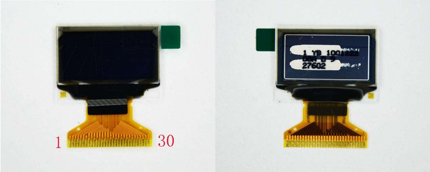
2.1 0.96 寸 OLED 裸屏外观
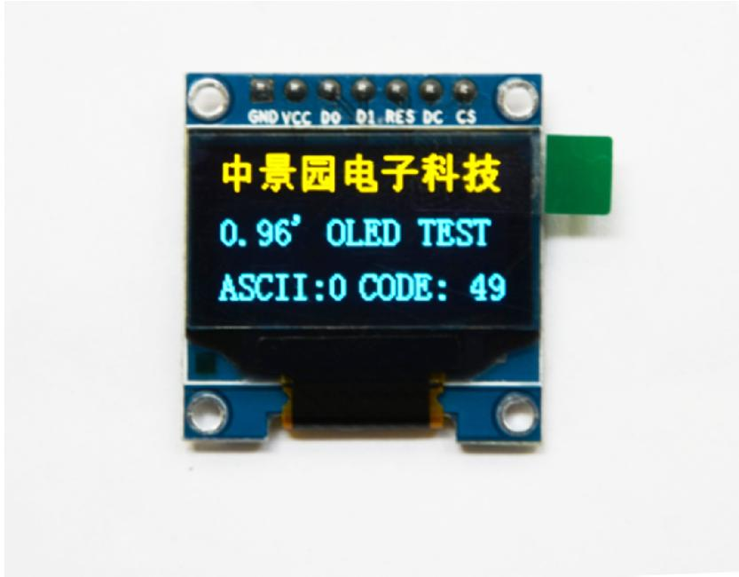
2.2 0.96 寸 OLED 模块
2.2.1 SPI/IIC 接口模块
模块接口定义:
1. GND 电源地
2. VCC 电源正(3~5.5V)
3. D0 OLED 的 D0 脚,在 SPI 和 IIC 通信中为时钟管脚
4. D1 OLED 的 D1 脚,在 SPI 和 IIC 通信中为数据管脚
5. RES OLED 的 RES#脚,用来复位(低电平复位)
6. DC OLED 的 D/C#E 脚,数据和命令控制管脚
7. CS OLED 的 CS#脚,也就是片选管脚
2.2.2 IIC接口模块
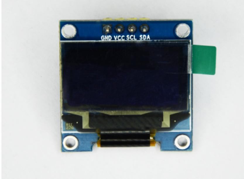
1. GND 电源地
2. VCC 电源正(3~5.5V)
3. SCL OLED 的 D0 脚,在 IIC 通信中为时钟管脚
4. SDA OLED 的 D1 脚,在 IIC 通信中为数据管脚
2.3 0.96 寸 OLED 驱动 IC
本屏所用的驱动 IC 为 SSD1306;其具有内部升压功能;所以在设计的时候不需要再专一设计 升压电路;当然了本屏也可以选用外部升压,具体的请详查数据手册。SSD1306 的每页包含了 128 个字节,总共 8 页,这样刚好是 128*64 的点阵大小。这点与 1.3 寸 OLED 驱动 IC SSD1106 稍有不同,SSD1106 每页是 132 个字节,也是 8 页。所以在用 0.96 寸 OLED 移植 1.3 寸 OLED 程 序的时候需要将 0.96 寸的显示地址向右偏移 2,这样显示就正常了;否则在用 1.3 寸的时候 1.3 寸屏右边会有 4 个像素点宽度显示不正常或是全白,这点大家注意一下。其它的 SSD1306 和 SSD1106 区别不大。
三、中景园电子 0.96 寸 OLED 模块使用方法
3.1 七针 SPI/IIC OLED 模块使用方法
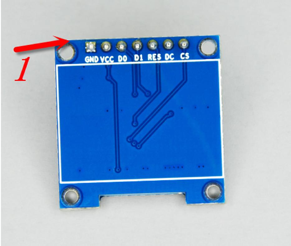
七针 SPI/IIC OLED 模块共有七个管脚,1~7 分别为 GDN、VCC、D0、D1、RES、DC、CS 此模块支持四线 SPI、三线 SPI、IIC 接口;由 OLED 的数据手册我们可以知道 0.96 寸 OLED 裸屏是 支持四种五种不同接口的;除了前面的三种还有 6800、8080 并口方式;由于这两种接口占用数 据 线 比 较 多 ; 而 且 不 太 常 用 , 所 以 模 块 在 设 计 的 时 候 没 有 引 出 来 。
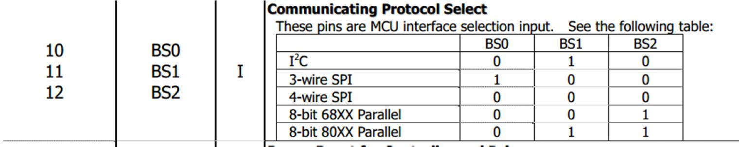
大家可以看出来;模块的通信接口是通过 BS0,BS1,BS2 三个管脚来配置的。
所设计的模块默认是 SPI 接口;
1. GND 电源地
2. VCC 电源正(3~5.5V)
3. D0 OLED 的 D0 脚,在 SPI 和 IIC 通信中为时钟管脚
4. D1 OLED 的 D1 脚,在 SPI 和 IIC 通信中为数据管脚
5. RES OLED 的 RES#脚,用来复位(低电平复位)
6. DC OLED 的 D/C#E 脚,数据和命令控制管脚
7. CS OLED 的 CS#脚,也就是片选管脚 大家在使用的时候一定注意,如下图所示。在 SPI 接口中 R1,R2,R8 三个电阻是不焊接的,如果大 家想用 IIC 接口的话需要将 R3 换到 R1 上,R8 可以焊接也可不焊接。
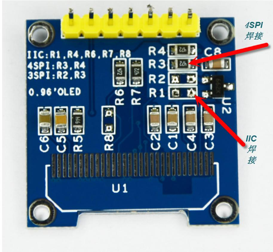
七针模块正面丝印如下,大家在接线的时候要注意不要接错了;特别是想用 IIC 接口的朋友们, 在 IIC 接口中需要将 RES 接高电平,可以与 VCC 对接,使 OLED 复位脚一直操持高电平,也就是不 复位的状态;同时需要将 DC,CS 接电源地;此时 IIC 通信中只需要 GND ,VCC,D0(时钟信号),D1(数 据信号)四根线了。如果大家感觉这样比较麻烦;建议大家直接选用四针的 IIC 接口模块。
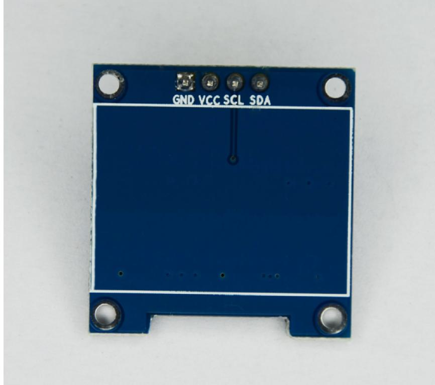
3.2 四针 IIC 接口模块使用说明
四针 iic 接口相对比较简单一些,只有两个信号线
1. GND 电源地
2. VCC 电源正(3~5.5V)
3. SCL OLED 的 D0 脚,在 IIC 通信中为时钟管脚
4. SDA OLED 的 D1 脚,在 IIC 通信中为数据管脚
四、0.96 寸 OLED 原理图设计注意事项

4.1 SPI 接口设计
在 SPI 接口中需保证 BS0,BS1,BS2 全为 0,也不是接地;所以在接口配置电阻中
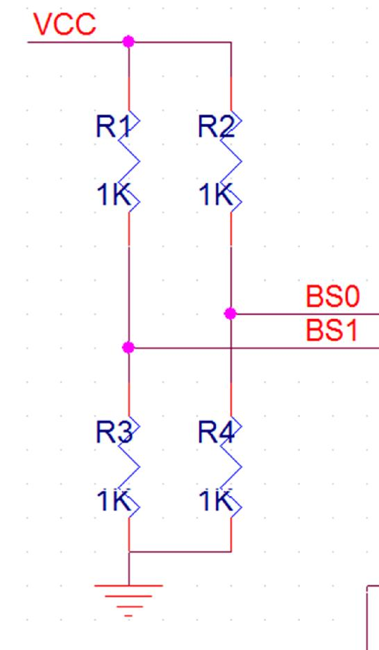
R1,R2 不焊接,R3,R4 焊接就可以了;同时电阻 R8 一 定不要焊接;否则会出现不稳定情况。 附加说明原理图中的 662K 为一 3.3v 的稳压管如果大家是直接用 3.3v 供电的话可以省去 662k。
4.2 IIC 接口设计
在 iic 接口中需要将 BS1 配置为 1,BS0 为 0;所以 R1,R4 焊接,R2,R3 不焊接,R8 可焊 接也可不焊接。
4.3 DIY 用户元件参数选择说明
对于 DIY 用户来说可能元件不像公司那么全;在设计的时候可能有些元件没有;需要用 其它参数的元件来拼凑;在 0.96OLED 中有几个参数比较重要;尽量搞成一样的
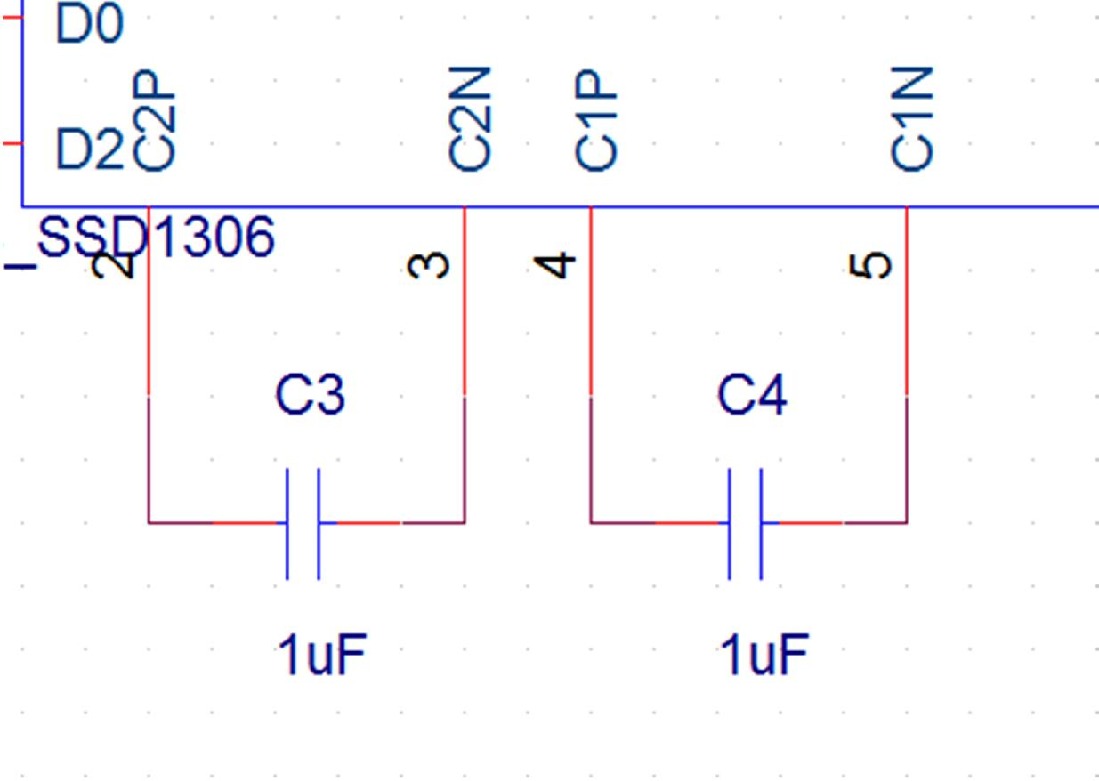
这里面的 C3,C4 在内部升压的时候要用;这两个参数尽量做到一样;都为 1uF;
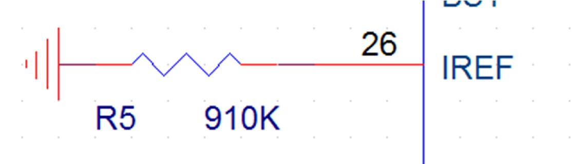
与 26 脚相连接的 910 电 阻 R5 的参数可以选在 1M 左右的;如果太小可能对屏的寿命有影响;如果太大屏的亮度会暗一 些;不过不影响使用。
五、关于不同平台的程序移植注意事项
很多新手工程师或是学生比较在意在某个处理器下的程序;其实这个没有必要;大家可以 打开几个不同平台下的程序,会发同一通信接口类型下的程序内部的操作函数是完全一样的,只 是管脚定义方式不同,还有一个就是需要包含所用平台的头文件;其它的其实都不用作修改;因 为其它的函数均是对 OLED 屏的操作;与所用的处理器平台没有关系。
因为大家对 C51 单片机相对都比较熟悉;大学里基本上都学习过;在此我以 C51 的程序来 作简单说明 ;大家在移植的时候尽量参考 C51 的程序。大家打开程序会发现主要有几人文件
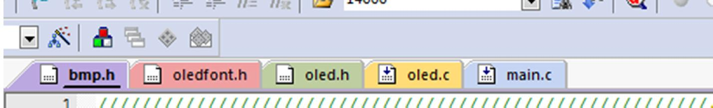
Bmp.h 是存放的图片数据,也就是大家对一 BMP 图片取模的数据
Oledfont.H 主要是存放的字库数据,包含常用的字符和用户自己所取模的中文
Oled.c 主要是函数的操作
Main.c 这个就不说了


 2439
2439

 被折叠的 条评论
为什么被折叠?
被折叠的 条评论
为什么被折叠?
 到【灌水乐园】发言


