


目录
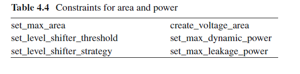
1.2 Constraints for Area and Power
1.3 Constraints for Design Rules
1.4 Constraints for Interfaces
1.5 Constraints for Specific Modes and Configurations
1.6 Exceptions to Design Constraints
5.1 Setup and Hold Timing check
1.SDC overview
The constrains in SDC format can be broadly categorized as:
1.Constraints for timing
2.Constraints for area and power
3.Constraints for design rules
4.Constrains for interfaces
5.Constrains for specific modes and configurations
6.Exceptions to design requirements
7.Miscellaneous commands
some of the Constraints can fall in more than one category
1.1 Constraints for Timing

create_clock [-period period_value] [source_objects] [-name clock_name] [-waveform edge_list] [-add] [-comment comment_string]
i.e
create_clock -name jtag_tck -period 100.00 -waveform {0 50} [get_ports PI_JTAG_TCK]
1.2 Constraints for Area and Power
1.3 Constraints for Design Rules

1.4 Constraints for Interfaces

1.5 Constraints for Specific Modes and Configurations

1.6 Exceptions to Design Constraints

1.7 Miscellaneous Commands

2. Design Query in SDC

3.create_clock
基本cmd:create_clock [-period period_value] [-name clock_name] [-waveform edge_list] [-add] [source_objects] [-comment comment_string]
To define a clock, we need to provide the following information:
1),Clock source: 来源可以是3个:(1) a port of the design[get_ports port_name];
(2) a cell inside the design[ get_pins pin_name];
(3) a net inside the design[get_net net_name];
在Fig5.4中,假设DFF 的clock周期为10,占空比40%,则clock可以设为:
(1)create_clock -name CLK -period 10 -waveform{0 4} [get_ports A]
(2)create_clock -name CLK -period 10 -waveform{0 4} [get_pins FF/P] FF是flop的名字;
(3)create_clock -name CLK -period 10 -waveform{0 4} [get_nets N]
i.e
create_clock -name jtag_tck -period 100.00 -waveform {0 50} [get_ports PI_JTAG_TCK] 
-name:用来命名CLK;
-period: 用来指定周期;
-wave{0 5}: 用来指定占空比,如果没有用-wave option,则占空比为50%;
-add:该参数用在当同一object有多个CLK 时使用;
在Fig.5.7中,CLK有两个source,C1和C2,C1周期是10ns,C2周期是15ns;This is represented as:
create_clock -name C1 -period 10 [get_ports CLK]
create_clock -name C2 -period 15 [get_ports CLK] -add
通过参数-add 在同一个port上设置多个CLK信息,在同一object上指定不同clk时,必须加上-name来命名不同clk,如果没有加-add参数,那么最后一个clock definition会覆盖前面的clock definition。
-comment: 该参数只是增加注释,对synthesis和timing没有影响,eg. create_clock -period 10 -name CLK [get_ports CLK] -comment "Clock for USB generated by PLL"
Virtual Clocks: 虚拟时钟应用场景,当某些block没有时钟时,designer需要在没有时钟的block中对ports/pins 下constrain。Virtual Clocks are modeled using the create_clock command with period,waveform,and name option only, but source object is missing. For example,
create_clock -period 10 -name v_clk -waveform{0 5} [get_ports clk]
4. generated clocks
由一个master clock derive出多个不同的clock,叫做generate clock或者derived clock,generated clock可以由如下方式产生:
1) Clock dividers
2) Clock multipliers
3) Clock gating
4.1 Clock Divider
Clock Divider 用来产生比source clock周期更大,频率更低的generated clock。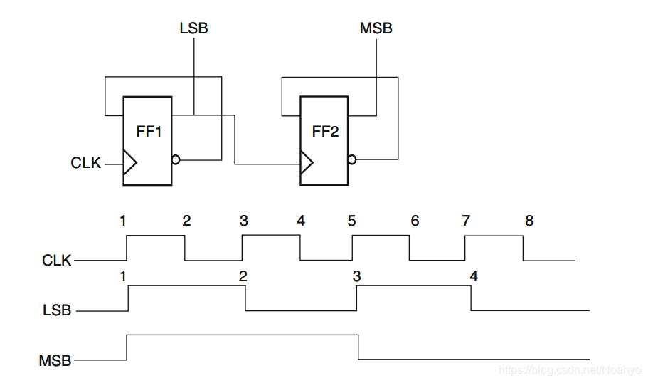
4.2 Clock Multipiler
Clock Multipiler用来产生比source clock周期更小,频率更快的generated clock.
下图CLKOUT 是CLK频率的两倍。
4.3 Clock Gating

4.4 Create_generated_clock
eg.
-source_objects: 指定design objects, 可以是port, pin,or net,source objects refers to the point where the generated clock(or clock) is being specified,
-source: 用来指定generated_clock的source pin,source of the generated clock refers to the point which acts as a reference from which the generated clock has been obtained
note: -source_objects和-source的区别,前者指指定generated clock的点,后者指获取generated clock的参考点。
-master_clock: 当一个clk ports可能有多个clock时,如Fig.5.7,那么generated clock需要用-master_clock参数来指定其来源于哪一个clock。
-name:用来指定generated clock的名字
-edges:表示generated clock的交替的rising edge和falling edge,必须包含至少3个整数,以用来表示generated clock一个完整的时钟周期。start with 1,代表source clock第一个rising edge.
-divide_by 2: 表示generated clock的频率被除以一个因素(factor),即周期乘以一个因素,此处为频率除以2
-multiple_by 2: 表示generated clock的频率被乘以一个因素,即周期除以一个因素。
create_clock -period 10 -name CLK[get_ports CLK]
created_generated_clock -name LSB -source [get_ports CLK] -divide_by 2 [get_pins FF1/Q]
created_generated_clock -name MSB -source [get_pins FF1/Q] -divide_by 2 [get_pins FF2/Q]
LSB和MSB也可以用-edges来描述
create_generated_clock -name LSB -source [get_ports CLK] -edges {1 3 5} [get_pins FF1/Q]
create_generated_clock -name MSB -source [get_pins FF1/Q] -edges{1 3 5} [get_pins FF2/Q]
由于MSB的source是LSB,所以-edges 是用LSB作为reference。
MSB也可以用CLK作为source,此时-edges {1 5 9}
create_generated_clock -name MSB -source [get_ports CLK] -edges {1 5 9 } [get_pins FF2/Q]

-invert: 用来将clock翻转。
在Fig.6.5中,divider is triggered by positive edge of CLK, GCLK1 is defined as:
create_generated_clock -name GCLK1 -source [get_ports CLK] -divide_by 2 [get_pins FF1/Q]
GCLK2 是GCLK1的inverterd version,GCLK2 is defined as:
create_generated_clock -name GCLK2 -source [get_ports CLK] -devide_by 2 -invert [get_pins FF1/QBAR]
在Fig.6.6中,divider is triggered by negetive edge of CLK, GCLK3 is defined as:
create_generated_clock -name GCLK3 -source [get_ports CLK] -edges {2 4 6} [get_pins FF1/Q]
GCLK4是GCLK3的inverted version, GCLK4 is defined as:
create_generated_clock -name GCLK4 -source [get_ports CLK] -edges {4 6 8} [get_pins FF1/QBAR]
-edge_shift: the edges of a generated clock may need to be moved by time units to indicate shift.
在Fig.6.4中,如果inverter chain的delay是2ns,那么PULSE can be defined as:
creater_generated_clock -name PULSE -source [get_ports CLK] -edges { 1 1 3} -edge_shift {0 2 0} [get_pins AN1/Z]
-duty_cycle:用来指定duty_cycle
-add :当同一个port上有多个CLK时,用-add option 定义多个clk
在Fig.6.7中,各个clock如下定义
create_clock -name C1 -period 10 [get_ports CLK]
create_clock -name C2 -period 15 [get_ports CLK] -add
#the following generated clock is based on C1's charateristics
create_generated_clock -name GC1 -divide_by 3 -source [get_ports CLK] -master_clock C1 [get_pins FF2/Q]
#the following generated clock is based on C2's charateristics
create_generated_clock -name GC2 -divide_by 3 -source [get_ports CLK] -master_clock C2 [get_pins FF2/Q]
-combinational
create_generated_clock -name CLKOUT -combinational -source [get_pins FF1/Q] [get_ports CLKOUT]
5 Clock Groups
5.1 Setup and Hold Timing check
setup : is defined as the time by which data needs to be available before the active edge of clock.
hold : is the time for which the data must remain stable after the active edge of clock.
假设:tF:delay from Clock to Q pin of flop(F1);
tC: delay within the combination cloud.T
因此data到达F2的时间是tF+tC.如果要满足setup check,则:![]()
如果要满足后来的check,则:
5.2 set_clock_group

-name: 指定clock group 独一无二的名字;
-group:列出group中的CLK;
-logically_exclusive:表示clock group 逻辑互斥;
-physically_exclusive:表示clock group物理互斥;
-asynchronous:表示clock group是异步的;
-allow_paths:
-comments: 增加注释;
clock group: 时钟组,定义完时钟后,需要通过设置clock group来确认各个时钟之间的关系。工具不会对处于不同clock group的时钟检查时序,因为我们通常需要做cross domain check(CDC check),如果clock group设错了,会导致整个STA检查错误。一般有三种clock group属性选择:
a) asynchronous: 代表两个asynchronous clock group,tool会做正常的SI分析
b) physically_exclusive:代表两个clock group在物理意义上互斥,比如在一个source pin上定义了两个时钟,这时候,工具会禁止分析。
c) logically_exclusive: 代表两个clock group在逻辑上互斥,比如两个clock经过MUX选择器。tool分析时,采用inifinite window(信号全部翻转),而不是看具体的timing window, 较为悲观。
(a) If two or more clocks coexits in the design,but there is no phase relationship, then they are specified as -asynchronous in set_clock_group.
(b) If two or more clocks coexits in the design,but there is a circuit to select only one among these,then they are specifed as -logically_exclusive in set_clock_group.
(c) If two or more clocks cannot coexit in the design, then they are specifed as -physically_exclusive in set_clock_group
eg: CLK1A和CLK1B是physically_exclusive; CLK1A和CLK2, CLK1B和CLK2, CLK3和CLK4是logically_exclusive; (都可以存在于Y端但却不能同时存在)
set_clock_group -name groupA -physically_exclusive -group"CLK1A" -group"CLK1B"
set_clock_group -name groupB -logically_exclusive -group"CLK1A CLK1B CLK3" -group "CLK2" -group "CLK4"
set_clock_group -name asysnc_group -asynchronous -group CLK1 -group CLK2
create_clock -period 10 -name C1 -waveform {0 5} [get_ports C1]
create_clock -period 20 -name C2 -waveform {0 12} [get_ports C2]
set_clock_groups -logically_exclusive -group C1 -group C2
可以在一个set_clock_groups 命令中加多个clk, i.e:
set_clock_groups -asynchronous -group [get_clocks {clk1 clk2 clk3}] -group [get_clocks{clk3 clk5 clkt}]
This command implies:
1. clk1 is asynchronous to clk4,clk5,clk6;
2. clk2 is asynchronous to clk4,clk5,clk6;
3. clk3 is asynchronous to clk4,clk5,clk6;
4. No relation can be assumed among clk1,clk2, and clk3.
5. No relation can be assumed among clk4,clk5, and clk6.
6.Other Clock Characteristics
6.1 Transition Time
Fig.8.1
slew: The rate of change of signal,通常是以信号从一种状态变为另一种状态所需的时间来衡量。上图如果以30%-70%作为测量阈值,那么Slew就是电压从30%到70%(对于理想状态下是信号从0变为1)所需要的时间,也称为transition Time。
set_clock_transition 来指定slew参数。
-rise:设置从0到1的rise transition time
-fall:设置从1到0的fall transition time
-max:设置最大transition time
-min:设置最小transition time
clock_list: 应该和用create_clock 或者create_generated_clock 设置的clock名字相匹配;
transition_time:设置transition 时间. eg
#Rise transition on Clock C1
create_clock -name C1_CLK
set_clock_transition -rise 0.2 C1_CLK
或者set_clock_transition -rise 0.2 [get_clocks C1_CLK]
#Fall transition on Clock C2 for min and max conditions
set_clock_transition -fall -min 0.2 [get_clocks C2]
set_clock_transition -fall -max 0.4 [get_clocks C2]
#Transition(rise,fall,min,max) on all clocks in the design
set_clock_transition 0.3 [all_clocks]
6.2 Skew and Jitter
skew: difference betweeen clock arrivals at different points in a design.
Jitter: undesired deviation in a periodicity of a clock.
skew和jitter一起造成的影响归类为Uncertainty.
Intraclock Uncertainty: same clock on source and destination;(clock的source和destination相同)
Interclock Uncertainty: source and destination having different clocks.


When modeling skew or jitter on a single clock (intraclock uncertainty), you need to specify the name of the clock, port or pin.
User can also specify different uncertainty values for setup and hold checks using -setup and -hold options.
For intraclock uncertainty, setup is impacted by both jitter and skew.While hold is impacted only by skew,not jitter. 所以通常setup的uncertainty要比hold的uncertainty 要大些。
eg. #Intraclock Uncertainty
set_clock_uncertainty 0.5 [get_clocks C1]
set_clock_uncertainty -setup 0.5 [get_clocks C2] (skew and jitter)
set_clock_uncertainty -hold 0.2 [get_clocks C2] (only skew)
#Clock uncertainty from C1 to C2 for setup and hold
set_clock_uncertainty -from C1 -to C2 -setup 0.5
set_clock_uncertainty -from C1 -to C2 -hold 0.2
#Clock uncertainty from rising edge (C1) to falling edge (C2)
set_clock_uncertainty -rise_from C1 -fall_to C2 0.5
在Fig.8.3中,there is a path from C1 to C2 and also a path from C2 to C1,所以需要specify 所有的clock path。
#Clock uncertainty between C1 and C2
set_clock_uncertainty -from C1 -to C2 0.5
set_clock_uncertainty -from C2 -to c1 0.5
当同时设了interclock 和intraclock,则interclock的优先级高
#Intraclock and Interclcok Uncertainty Conflict
set_clock_uncertainty 0.6 -from C2 -to C1
set_clock_uncertainty 0.5 [get_clocks C1]
For all paths from C2 to C1, the interclock uncertainty takes precedence, and a value of 0.6 is used.
For all other paths where the destination clock is C1, the intraclock value of 0.5 is used.
6.3 Clock Latency
clock Latency:The delay between the source of the clock and the actual pin where clock is used to trigger a device is defeind as clock latency.
clock latency可分为souce latency和network latency:
- source latency是这clock 信号源 到芯片的clock输入端的delay;
- network latency是指芯片clokc输入端到flip-flop时钟输入端的delay


8.4.a set_clock_latency -source 0.5 [get_clocks C1]
7 Port Delays
需要对input output pins设delays,如果不设的话,timing analysis tool就会认为interfaces上时序非常乐观,combinatinonal logic会被假定会占用整个时钟周期,而不会对外部模块留有clk余地。


 212
212


 被折叠的 条评论
为什么被折叠?
被折叠的 条评论
为什么被折叠?
 到【灌水乐园】发言


