


09 STM32F429 RCC时钟
对时钟树流程的简单理解
时钟树图
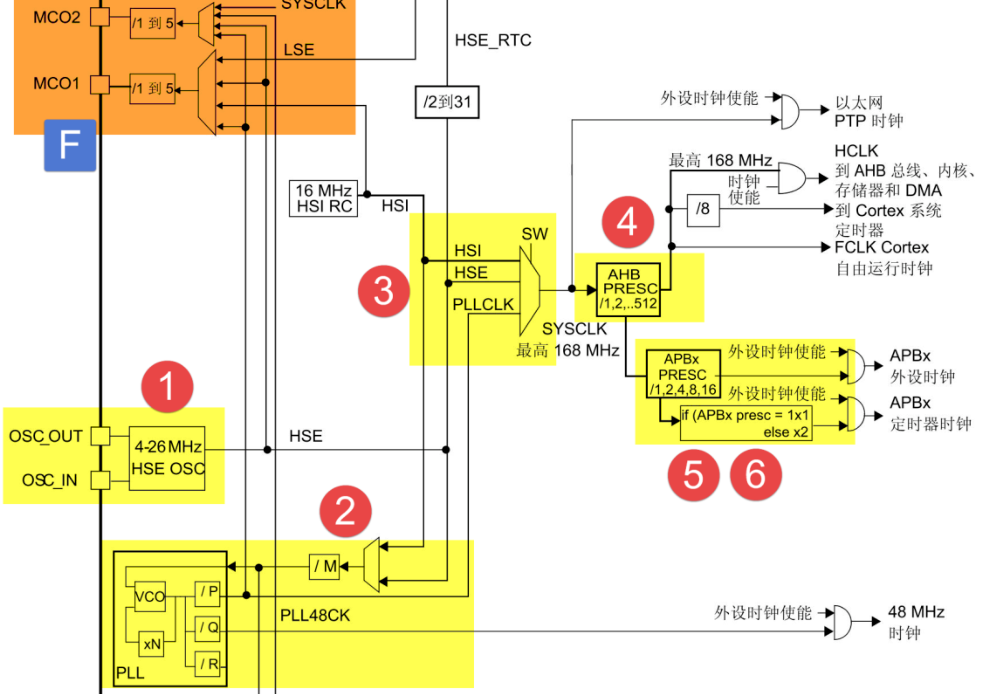
-
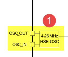
HSE是高速外部时钟信号, HSI是高速内部时钟信号,通常使用HSE,因为HSI在内部受温度等影响不稳定
-
HSE的频率一般为8MHZ,使用RCC_CR的16位进行使能,17位读取时钟是否已经就绪
RCC基地址

RCC_CR寄存器
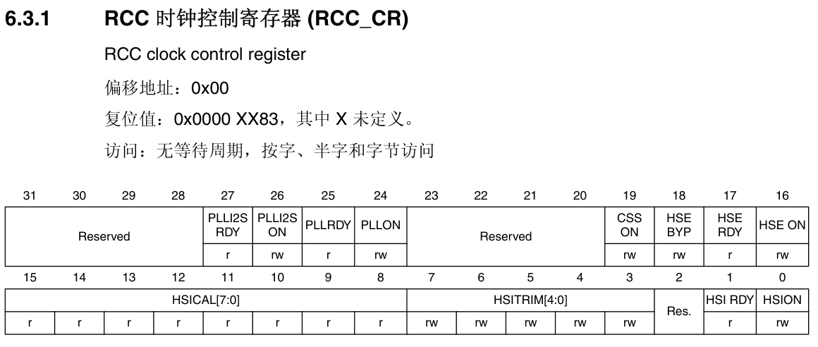
判断HSE是否启动成功
 __IO uint32_t StartUpCounter = 0, HSEStatus = 0;

  /* Enable HSE */
  RCC->CR |= ((uint32_t)RCC_CR_HSEON);

  /* Wait till HSE is ready and if Time out is reached exit */
  do
  {
    HSEStatus = RCC->CR & RCC_CR_HSERDY;
    StartUpCounter++;
  } while((HSEStatus == 0) && (StartUpCounter != HSE_STARTUP_TIMEOUT));

  if ((RCC->CR & RCC_CR_HSERDY) != RESET)
  {
    HSEStatus = (uint32_t)0x01;
  }
  else
  {
    HSEStatus = (uint32_t)0x00;
  }
RCC_CFGR寄存器
[外链图片转存失败,源站可能有防盗链机制,建议将图片保存下来直接上传(img-fCU9wNne-1664218657494)(https://picture-1309470925.cos.ap-chengdu.myqcloud.com/pic/image-20220926232933972.png)]
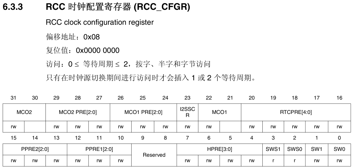
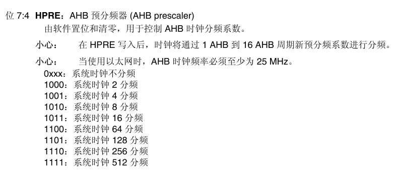
启动成功之后总线分频配置代码如下
    /* HCLK = SYSCLK / 1*/
    RCC->CFGR |= RCC_CFGR_HPRE_DIV1;

    /* PCLK2 = HCLK / 2*/
    RCC->CFGR |= RCC_CFGR_PPRE2_DIV2;

    /* PCLK1 = HCLK / 4*/
    RCC->CFGR |= RCC_CFGR_PPRE1_DIV4;
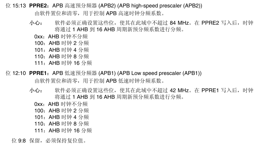
RCC PLL 配置寄存器
设置锁相环
[外链图片转存失败,源站可能有防盗链机制,建议将图片保存下来直接上传(img-M3eqhtBb-1664218657496)(https://picture-1309470925.cos.ap-chengdu.myqcloud.com/pic/image-20220926234025936.png)]
    /* Configure the main PLL */
    RCC->PLLCFGR = PLL_M | (PLL_N << 6) | (((PLL_P >> 1) -1) << 16) |
                   (RCC_PLLCFGR_PLLSRC_HSE) | (PLL_Q << 24);

    /* Enable the main PLL */
    RCC->CR |= RCC_CR_PLLON;

    /* Wait till the main PLL is ready */
    while((RCC->CR & RCC_CR_PLLRDY) == 0)
    {
    }
这里为RCC_CFGR配置,选择锁相环时钟
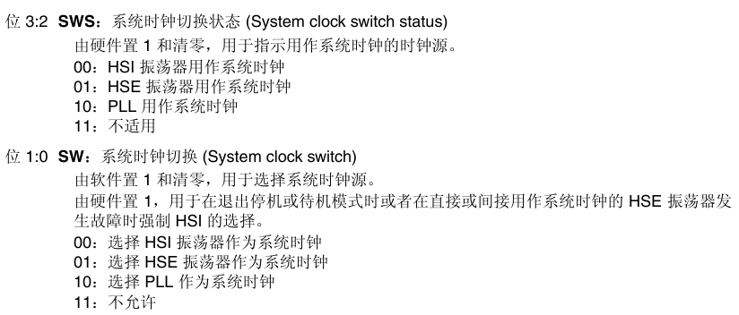
 /* Select the main PLL as system clock source */
    RCC->CFGR &= (uint32_t)((uint32_t)~(RCC_CFGR_SW));
    RCC->CFGR |= RCC_CFGR_SW_PLL;

    /* Wait till the main PLL is used as system clock source */
    while ((RCC->CFGR & (uint32_t)RCC_CFGR_SWS ) != RCC_CFGR_SWS_PLL);
    {
    }
精简后的代码
原版
#include "bsp_rcc.h"

static void SetSysClock(void)
{
  __IO uint32_t StartUpCounter = 0, HSEStatus = 0;

  /* 1--------Enable HSE----------*/
  RCC->CR |= ((uint32_t)RCC_CR_HSEON);

  /* Wait till HSE is ready and if Time out is reached exit */
  do
  {
    HSEStatus = RCC->CR & RCC_CR_HSERDY;
    StartUpCounter++;
  } while((HSEStatus == 0) && (StartUpCounter != HSE_STARTUP_TIMEOUT));

  if ((RCC->CR & RCC_CR_HSERDY) != RESET)
  {
    HSEStatus = (uint32_t)0x01;
  }
  else
  {
    HSEStatus = (uint32_t)0x00;
  }

	/* 2--------HSE启动成功,配置AHB APB1 APB2的分频因子----------*/
  if (HSEStatus == (uint32_t)0x01)
  {
    /* Select regulator voltage output Scale 1 mode */
    RCC->APB1ENR |= RCC_APB1ENR_PWREN;
    PWR->CR |= PWR_CR_VOS;

    /* HCLK = SYSCLK / 1*/
    RCC->CFGR |= RCC_CFGR_HPRE_DIV1;

    /* PCLK2 = HCLK / 2*/
    RCC->CFGR |= RCC_CFGR_PPRE2_DIV2;

    /* PCLK1 = HCLK / 4*/
    RCC->CFGR |= RCC_CFGR_PPRE1_DIV4;

    	/* 3.--------配置PLL的各项分频因子,并使能----------*/
    RCC->PLLCFGR = PLL_M | (PLL_N << 6) | (((PLL_P >> 1) -1) << 16) |
                   (RCC_PLLCFGR_PLLSRC_HSE) | (PLL_Q << 24);

    /* Enable the main PLL */
    RCC->CR |= RCC_CR_PLLON;

    /* Wait till the main PLL is ready */
    while((RCC->CR & RCC_CR_PLLRDY) == 0)
    {
    }

    /* Enable the Over-drive to extend the clock frequency to 180 Mhz */
    PWR->CR |= PWR_CR_ODEN;
    while((PWR->CSR & PWR_CSR_ODRDY) == 0)
    {
    }
    PWR->CR |= PWR_CR_ODSWEN;
    while((PWR->CSR & PWR_CSR_ODSWRDY) == 0)
    {
    }
    /* Configure Flash prefetch, Instruction cache, Data cache and wait state */
    FLASH->ACR = FLASH_ACR_PRFTEN | FLASH_ACR_ICEN |FLASH_ACR_DCEN |FLASH_ACR_LATENCY_5WS;

    	/* 4.--------选择系统时钟,这里是使用PLL时钟----------*/
    RCC->CFGR &= (uint32_t)((uint32_t)~(RCC_CFGR_SW));
    RCC->CFGR |= RCC_CFGR_SW_PLL;

    /* Wait till the main PLL is used as system clock source */
    while ((RCC->CFGR & (uint32_t)RCC_CFGR_SWS ) != RCC_CFGR_SWS_PLL);
    {
    }
  }
  else
  { /* If HSE fails to start-up, the application will have wrong clock
         configuration. User can add here some code to deal with this error */
  }
}
使用固件库编程
/*使用固件库超频
m: 2-63
n: 192-432
p: 2,4,6,8
q: 2-15
SYSCLK = (HSE/m)*n/p = 25/25*432/2=216M
*/
void HSE_SetSysClock(uint32_t m ,uint32_t n,uint32_t p,uint32_t q){
	uint32_t HSEStartupStatus = 0;
	//使能HSE
	RCC_HSEConfig(RCC_HSE_ON);
	//检测HSE是否已经启动成功
	HSEStartupStatus = RCC_WaitForHSEStartUp();
	if(HSEStartupStatus == SUCCESS){
		/* 选择电压调节器件,输出模式为1 */
		/* 使能电源使能时钟*/
    RCC->APB1ENR |= RCC_APB1ENR_PWREN;
    PWR->CR |= PWR_CR_VOS;

		RCC_HCLKConfig(RCC_SYSCLK_Div1);
		RCC_PCLK1Config(RCC_SYSCLK_Div4);
		RCC_PCLK2Config(RCC_SYSCLK_Div2);
		//设置PLL锁相环
		RCC_PLLConfig(RCC_PLLSource_HSE,m,n,p,q);
		//使能PPL
		RCC_PLLCmd(ENABLE);
		//检验是否已经使能
		while(RCC_GetFlagStatus(RCC_FLAG_PLLRDY) == RESET){}
		/* Enable the Over-drive to extend the clock frequency to 180 Mhz */
    PWR->CR |= PWR_CR_ODEN;
    while((PWR->CSR & PWR_CSR_ODRDY) == 0)
    {
    }
    PWR->CR |= PWR_CR_ODSWEN;
    while((PWR->CSR & PWR_CSR_ODSWRDY) == 0)
    {
    }
    /* Configure Flash prefetch, Instruction cache, Data cache and wait state */
    FLASH->ACR = FLASH_ACR_PRFTEN | FLASH_ACR_ICEN |FLASH_ACR_DCEN |FLASH_ACR_LATENCY_5WS;

		RCC_SYSCLKConfig(RCC_SYSCLKSource_PLLCLK);
	}
	else{//启动失败,添加纠错代码

	}

}
/**
  * @brief  Configures the External High Speed oscillator (HSE).
  * @note   After enabling the HSE (RCC_HSE_ON or RCC_HSE_Bypass), the application
  *         software should wait on HSERDY flag to be set indicating that HSE clock
  *         is stable and can be used to clock the PLL and/or system clock.
  * @note   HSE state can not be changed if it is used directly or through the
  *         PLL as system clock. In this case, you have to select another source
  *         of the system clock then change the HSE state (ex. disable it).
  * @note   The HSE is stopped by hardware when entering STOP and STANDBY modes.
  * @note   This function reset the CSSON bit, so if the Clock security system(CSS)
  *         was previously enabled you have to enable it again after calling this
  *         function.
  * @param  RCC_HSE: specifies the new state of the HSE.
  *          This parameter can be one of the following values:
  *            @arg RCC_HSE_OFF: turn OFF the HSE oscillator, HSERDY flag goes low after
  *                              6 HSE oscillator clock cycles.
  *            @arg RCC_HSE_ON: turn ON the HSE oscillator
  *            @arg RCC_HSE_Bypass: HSE oscillator bypassed with external clock
  * @retval None
  */
void RCC_HSEConfig(uint8_t RCC_HSE)
{
  /* Check the parameters */
  assert_param(IS_RCC_HSE(RCC_HSE));

  /* Reset HSEON and HSEBYP bits before configuring the HSE ------------------*/
  *(__IO uint8_t *) CR_BYTE3_ADDRESS = RCC_HSE_OFF;

  /* Set the new HSE configuration -------------------------------------------*/
  *(__IO uint8_t *) CR_BYTE3_ADDRESS = RCC_HSE;
}


/**
  * @brief  Waits for HSE start-up.
  * @note   This functions waits on HSERDY flag to be set and return SUCCESS if
  *         this flag is set, otherwise returns ERROR if the timeout is reached
  *         and this flag is not set. The timeout value is defined by the constant
  *         HSE_STARTUP_TIMEOUT in stm32f4xx.h file. You can tailor it depending
  *         on the HSE crystal used in your application.
  * @param  None
  * @retval An ErrorStatus enumeration value:
  *          - SUCCESS: HSE oscillator is stable and ready to use
  *          - ERROR: HSE oscillator not yet ready
  */
ErrorStatus RCC_WaitForHSEStartUp(void)
{
  __IO uint32_t startupcounter = 0;
  ErrorStatus status = ERROR;
  FlagStatus hsestatus = RESET;
  /* Wait till HSE is ready and if Time out is reached exit */
  do
  {
    hsestatus = RCC_GetFlagStatus(RCC_FLAG_HSERDY);
    startupcounter++;
  } while((startupcounter != HSE_STARTUP_TIMEOUT) && (hsestatus == RESET));

  if (RCC_GetFlagStatus(RCC_FLAG_HSERDY) != RESET)
  {
    status = SUCCESS;
  }
  else
  {
    status = ERROR;
  }
  return (status);
}

void RCC_PLLConfig(uint32_t RCC_PLLSource, uint32_t PLLM, uint32_t PLLN, uint32_t PLLP, uint32_t PLLQ)
{
  /* Check the parameters */
  assert_param(IS_RCC_PLL_SOURCE(RCC_PLLSource));
  assert_param(IS_RCC_PLLM_VALUE(PLLM));
  assert_param(IS_RCC_PLLN_VALUE(PLLN));
  assert_param(IS_RCC_PLLP_VALUE(PLLP));
  assert_param(IS_RCC_PLLQ_VALUE(PLLQ));

  RCC->PLLCFGR = PLLM | (PLLN << 6) | (((PLLP >> 1) -1) << 16) | (RCC_PLLSource) |
                 (PLLQ << 24);
}

/**
  * @brief  Configures the system clock (SYSCLK).
  * @note   The HSI is used (enabled by hardware) as system clock source after
  *         startup from Reset, wake-up from STOP and STANDBY mode, or in case
  *         of failure of the HSE used directly or indirectly as system clock
  *         (if the Clock Security System CSS is enabled).
  * @note   A switch from one clock source to another occurs only if the target
  *         clock source is ready (clock stable after startup delay or PLL locked).
  *         If a clock source which is not yet ready is selected, the switch will
  *         occur when the clock source will be ready.
  *         You can use RCC_GetSYSCLKSource() function to know which clock is
  *         currently used as system clock source.
  * @param  RCC_SYSCLKSource: specifies the clock source used as system clock.
  *          This parameter can be one of the following values:
  *            @arg RCC_SYSCLKSource_HSI: HSI selected as system clock source
  *            @arg RCC_SYSCLKSource_HSE: HSE selected as system clock source
  *            @arg RCC_SYSCLKSource_PLLCLK: PLL selected as system clock source (RCC_SYSCLKSource_PLLPCLK for STM32F446xx devices)
  *            @arg RCC_SYSCLKSource_PLLRCLK: PLL R selected as system clock source only for STM32F412xG, STM32F413_423xx and STM32F446xx devices
  * @retval None
  */
void RCC_SYSCLKConfig(uint32_t RCC_SYSCLKSource)
{
  uint32_t tmpreg = 0;

  /* Check the parameters */
  assert_param(IS_RCC_SYSCLK_SOURCE(RCC_SYSCLKSource));

  tmpreg = RCC->CFGR;

  /* Clear SW[1:0] bits */
  tmpreg &= ~RCC_CFGR_SW;

  /* Set SW[1:0] bits according to RCC_SYSCLKSource value */
  tmpreg |= RCC_SYSCLKSource;

  /* Store the new value */
  RCC->CFGR = tmpreg;
}
源代码流程
在项目启动的时候
Reset_Handler    PROC
                 EXPORT  Reset_Handler             [WEAK]
        IMPORT  SystemInit
        IMPORT  __main

                 LDR     R0, =SystemInit
                 BLX     R0
                 LDR     R0, =__main
                 BX      R0
                 ENDP
找到SystemInit函数的原型
void SystemInit(void)
{
  /* FPU settings ------------------------------------------------------------*/
  #if (__FPU_PRESENT == 1) && (__FPU_USED == 1)
    SCB->CPACR |= ((3UL << 10*2)|(3UL << 11*2));  /* set CP10 and CP11 Full Access */
  #endif
  /* Reset the RCC clock configuration to the default reset state ------------*/
  /* Set HSION bit */
  RCC->CR |= (uint32_t)0x00000001;

  /* Reset CFGR register */
  RCC->CFGR = 0x00000000;

  /* Reset HSEON, CSSON and PLLON bits */
  RCC->CR &= (uint32_t)0xFEF6FFFF;

  /* Reset PLLCFGR register */
  RCC->PLLCFGR = 0x24003010;

  /* Reset HSEBYP bit */
  RCC->CR &= (uint32_t)0xFFFBFFFF;

  /* Disable all interrupts */
  RCC->CIR = 0x00000000;

#if defined(DATA_IN_ExtSRAM) || defined(DATA_IN_ExtSDRAM)
  SystemInit_ExtMemCtl();
#endif /* DATA_IN_ExtSRAM || DATA_IN_ExtSDRAM */

  /* Configure the System clock source, PLL Multiplier and Divider factors,
     AHB/APBx prescalers and Flash settings ----------------------------------*/
  SetSysClock();

  /* Configure the Vector Table location add offset address ------------------*/
#ifdef VECT_TAB_SRAM
  SCB->VTOR = SRAM_BASE | VECT_TAB_OFFSET; /* Vector Table Relocation in Internal SRAM */
#else
  SCB->VTOR = FLASH_BASE | VECT_TAB_OFFSET; /* Vector Table Relocation in Internal FLASH */
#endif
}
其中的SetSysClock()函数是关键
static void SetSysClock(void)
{
#if defined(STM32F40_41xxx) || defined(STM32F427_437xx) || defined(STM32F429_439xx) || defined(STM32F401xx) || defined(STM32F412xG) || defined(STM32F413_423xx) || defined(STM32F446xx)|| defined(STM32F469_479xx)
/******************************************************************************/
/*            PLL (clocked by HSE) used as System clock source                */
/******************************************************************************/
  __IO uint32_t StartUpCounter = 0, HSEStatus = 0;

  /* Enable HSE */
  RCC->CR |= ((uint32_t)RCC_CR_HSEON);

  /* Wait till HSE is ready and if Time out is reached exit */
  do
  {
    HSEStatus = RCC->CR & RCC_CR_HSERDY;
    StartUpCounter++;
  } while((HSEStatus == 0) && (StartUpCounter != HSE_STARTUP_TIMEOUT));

  if ((RCC->CR & RCC_CR_HSERDY) != RESET)
  {
    HSEStatus = (uint32_t)0x01;
  }
  else
  {
    HSEStatus = (uint32_t)0x00;
  }

  if (HSEStatus == (uint32_t)0x01)
  {
    /* Select regulator voltage output Scale 1 mode */
    RCC->APB1ENR |= RCC_APB1ENR_PWREN;
    PWR->CR |= PWR_CR_VOS;

    /* HCLK = SYSCLK / 1*/
    RCC->CFGR |= RCC_CFGR_HPRE_DIV1;

#if defined(STM32F40_41xxx) || defined(STM32F427_437xx) || defined(STM32F429_439xx) ||  defined(STM32F412xG) || defined(STM32F446xx) || defined(STM32F469_479xx)
    /* PCLK2 = HCLK / 2*/
    RCC->CFGR |= RCC_CFGR_PPRE2_DIV2;

    /* PCLK1 = HCLK / 4*/
    RCC->CFGR |= RCC_CFGR_PPRE1_DIV4;
#endif /* STM32F40_41xxx || STM32F427_437x || STM32F429_439xx  || STM32F412xG || STM32F446xx || STM32F469_479xx */

#if defined(STM32F401xx) || defined(STM32F413_423xx)
    /* PCLK2 = HCLK / 1*/
    RCC->CFGR |= RCC_CFGR_PPRE2_DIV1;

    /* PCLK1 = HCLK / 2*/
    RCC->CFGR |= RCC_CFGR_PPRE1_DIV2;
#endif /* STM32F401xx || STM32F413_423xx */

#if defined(STM32F40_41xxx) || defined(STM32F427_437xx) || defined(STM32F429_439xx) || defined(STM32F401xx) || defined(STM32F469_479xx)
    /* Configure the main PLL */
    RCC->PLLCFGR = PLL_M | (PLL_N << 6) | (((PLL_P >> 1) -1) << 16) |
                   (RCC_PLLCFGR_PLLSRC_HSE) | (PLL_Q << 24);
#endif /* STM32F40_41xxx || STM32F401xx || STM32F427_437x || STM32F429_439xx || STM32F469_479xx */

#if  defined(STM32F412xG) || defined(STM32F413_423xx) || defined(STM32F446xx)
    /* Configure the main PLL */
    RCC->PLLCFGR = PLL_M | (PLL_N << 6) | (((PLL_P >> 1) -1) << 16) |
                   (RCC_PLLCFGR_PLLSRC_HSE) | (PLL_Q << 24) | (PLL_R << 28);
#endif /* STM32F412xG || STM32F413_423xx || STM32F446xx */

    /* Enable the main PLL */
    RCC->CR |= RCC_CR_PLLON;

    /* Wait till the main PLL is ready */
    while((RCC->CR & RCC_CR_PLLRDY) == 0)
    {
    }

#if defined(STM32F427_437xx) || defined(STM32F429_439xx) || defined(STM32F446xx) || defined(STM32F469_479xx)
    /* Enable the Over-drive to extend the clock frequency to 180 Mhz */
    PWR->CR |= PWR_CR_ODEN;
    while((PWR->CSR & PWR_CSR_ODRDY) == 0)
    {
    }
    PWR->CR |= PWR_CR_ODSWEN;
    while((PWR->CSR & PWR_CSR_ODSWRDY) == 0)
    {
    }
    /* Configure Flash prefetch, Instruction cache, Data cache and wait state */
    FLASH->ACR = FLASH_ACR_PRFTEN | FLASH_ACR_ICEN |FLASH_ACR_DCEN |FLASH_ACR_LATENCY_5WS;
#endif /* STM32F427_437x || STM32F429_439xx || STM32F446xx || STM32F469_479xx */

#if defined(STM32F40_41xxx)  || defined(STM32F412xG)
    /* Configure Flash prefetch, Instruction cache, Data cache and wait state */
    FLASH->ACR = FLASH_ACR_PRFTEN | FLASH_ACR_ICEN |FLASH_ACR_DCEN |FLASH_ACR_LATENCY_5WS;
#endif /* STM32F40_41xxx  || STM32F412xG */

#if defined(STM32F413_423xx)
    /* Configure Flash prefetch, Instruction cache, Data cache and wait state */
    FLASH->ACR = FLASH_ACR_PRFTEN | FLASH_ACR_ICEN |FLASH_ACR_DCEN |FLASH_ACR_LATENCY_3WS;
#endif /* STM32F413_423xx */

#if defined(STM32F401xx)
    /* Configure Flash prefetch, Instruction cache, Data cache and wait state */
    FLASH->ACR = FLASH_ACR_PRFTEN | FLASH_ACR_ICEN |FLASH_ACR_DCEN |FLASH_ACR_LATENCY_2WS;
#endif /* STM32F401xx */

    /* Select the main PLL as system clock source */
    RCC->CFGR &= (uint32_t)((uint32_t)~(RCC_CFGR_SW));
    RCC->CFGR |= RCC_CFGR_SW_PLL;

    /* Wait till the main PLL is used as system clock source */
    while ((RCC->CFGR & (uint32_t)RCC_CFGR_SWS ) != RCC_CFGR_SWS_PLL);
    {
    }
  }
  else
  { /* If HSE fails to start-up, the application will have wrong clock
         configuration. User can add here some code to deal with this error */
  }
#elif defined(STM32F410xx) || defined(STM32F411xE)
#if defined(USE_HSE_BYPASS)
/******************************************************************************/
/*            PLL (clocked by HSE) used as System clock source                */
/******************************************************************************/
  __IO uint32_t StartUpCounter = 0, HSEStatus = 0;

  /* Enable HSE and HSE BYPASS */
  RCC->CR |= ((uint32_t)RCC_CR_HSEON | RCC_CR_HSEBYP);

  /* Wait till HSE is ready and if Time out is reached exit */
  do
  {
    HSEStatus = RCC->CR & RCC_CR_HSERDY;
    StartUpCounter++;
  } while((HSEStatus == 0) && (StartUpCounter != HSE_STARTUP_TIMEOUT));

  if ((RCC->CR & RCC_CR_HSERDY) != RESET)
  {
    HSEStatus = (uint32_t)0x01;
  }
  else
  {
    HSEStatus = (uint32_t)0x00;
  }

  if (HSEStatus == (uint32_t)0x01)
  {
    /* Select regulator voltage output Scale 1 mode */
    RCC->APB1ENR |= RCC_APB1ENR_PWREN;
    PWR->CR |= PWR_CR_VOS;

    /* HCLK = SYSCLK / 1*/
    RCC->CFGR |= RCC_CFGR_HPRE_DIV1;

    /* PCLK2 = HCLK / 2*/
    RCC->CFGR |= RCC_CFGR_PPRE2_DIV1;

    /* PCLK1 = HCLK / 4*/
    RCC->CFGR |= RCC_CFGR_PPRE1_DIV2;

    /* Configure the main PLL */
    RCC->PLLCFGR = PLL_M | (PLL_N << 6) | (((PLL_P >> 1) -1) << 16) |
                   (RCC_PLLCFGR_PLLSRC_HSE) | (PLL_Q << 24);

    /* Enable the main PLL */
    RCC->CR |= RCC_CR_PLLON;

    /* Wait till the main PLL is ready */
    while((RCC->CR & RCC_CR_PLLRDY) == 0)
    {
    }

    /* Configure Flash prefetch, Instruction cache, Data cache and wait state */
    FLASH->ACR = FLASH_ACR_PRFTEN | FLASH_ACR_ICEN |FLASH_ACR_DCEN |FLASH_ACR_LATENCY_2WS;

    /* Select the main PLL as system clock source */
    RCC->CFGR &= (uint32_t)((uint32_t)~(RCC_CFGR_SW));
    RCC->CFGR |= RCC_CFGR_SW_PLL;

    /* Wait till the main PLL is used as system clock source */
    while ((RCC->CFGR & (uint32_t)RCC_CFGR_SWS ) != RCC_CFGR_SWS_PLL);
    {
    }
  }
  else
  { /* If HSE fails to start-up, the application will have wrong clock
         configuration. User can add here some code to deal with this error */
  }
#else /* HSI will be used as PLL clock source */
  /* Select regulator voltage output Scale 1 mode */
  RCC->APB1ENR |= RCC_APB1ENR_PWREN;
  PWR->CR |= PWR_CR_VOS;

  /* HCLK = SYSCLK / 1*/
  RCC->CFGR |= RCC_CFGR_HPRE_DIV1;

  /* PCLK2 = HCLK / 2*/
  RCC->CFGR |= RCC_CFGR_PPRE2_DIV1;

  /* PCLK1 = HCLK / 4*/
  RCC->CFGR |= RCC_CFGR_PPRE1_DIV2;

  /* Configure the main PLL */
  RCC->PLLCFGR = PLL_M | (PLL_N << 6) | (((PLL_P >> 1) -1) << 16) | (PLL_Q << 24);

  /* Enable the main PLL */
  RCC->CR |= RCC_CR_PLLON;

  /* Wait till the main PLL is ready */
  while((RCC->CR & RCC_CR_PLLRDY) == 0)
  {
  }

  /* Configure Flash prefetch, Instruction cache, Data cache and wait state */
  FLASH->ACR = FLASH_ACR_PRFTEN | FLASH_ACR_ICEN |FLASH_ACR_DCEN |FLASH_ACR_LATENCY_2WS;

  /* Select the main PLL as system clock source */
  RCC->CFGR &= (uint32_t)((uint32_t)~(RCC_CFGR_SW));
  RCC->CFGR |= RCC_CFGR_SW_PLL;

  /* Wait till the main PLL is used as system clock source */
  while ((RCC->CFGR & (uint32_t)RCC_CFGR_SWS ) != RCC_CFGR_SWS_PLL);
  {
  }
#endif /* USE_HSE_BYPASS */
#endif /* STM32F40_41xxx || STM32F427_437xx || STM32F429_439xx || STM32F401xx || STM32F469_479xx */
}
因为不使用有源晶振(价格昂贵),精简上面的代码,并且只留下与429相关的
#include "bsp_rcc.h"

static void SetSysClock(void)
{
  __IO uint32_t StartUpCounter = 0, HSEStatus = 0;

  /* Enable HSE */
  RCC->CR |= ((uint32_t)RCC_CR_HSEON);

  /* Wait till HSE is ready and if Time out is reached exit */
  do
  {
    HSEStatus = RCC->CR & RCC_CR_HSERDY;
    StartUpCounter++;
  } while((HSEStatus == 0) && (StartUpCounter != HSE_STARTUP_TIMEOUT));

  if ((RCC->CR & RCC_CR_HSERDY) != RESET)
  {
    HSEStatus = (uint32_t)0x01;
  }
  else
  {
    HSEStatus = (uint32_t)0x00;
  }

  if (HSEStatus == (uint32_t)0x01)
  {
    /* Select regulator voltage output Scale 1 mode */
    RCC->APB1ENR |= RCC_APB1ENR_PWREN;
    PWR->CR |= PWR_CR_VOS;

    /* HCLK = SYSCLK / 1*/
    RCC->CFGR |= RCC_CFGR_HPRE_DIV1;

    /* PCLK2 = HCLK / 2*/
    RCC->CFGR |= RCC_CFGR_PPRE2_DIV2;

    /* PCLK1 = HCLK / 4*/
    RCC->CFGR |= RCC_CFGR_PPRE1_DIV4;

    /* Configure the main PLL */
    RCC->PLLCFGR = PLL_M | (PLL_N << 6) | (((PLL_P >> 1) -1) << 16) |
                   (RCC_PLLCFGR_PLLSRC_HSE) | (PLL_Q << 24);

    /* Enable the main PLL */
    RCC->CR |= RCC_CR_PLLON;

    /* Wait till the main PLL is ready */
    while((RCC->CR & RCC_CR_PLLRDY) == 0)
    {
    }

    /* Enable the Over-drive to extend the clock frequency to 180 Mhz */
    PWR->CR |= PWR_CR_ODEN;
    while((PWR->CSR & PWR_CSR_ODRDY) == 0)
    {
    }
    PWR->CR |= PWR_CR_ODSWEN;
    while((PWR->CSR & PWR_CSR_ODSWRDY) == 0)
    {
    }
    /* Configure Flash prefetch, Instruction cache, Data cache and wait state */
    FLASH->ACR = FLASH_ACR_PRFTEN | FLASH_ACR_ICEN |FLASH_ACR_DCEN |FLASH_ACR_LATENCY_5WS;

    /* Select the main PLL as system clock source */
    RCC->CFGR &= (uint32_t)((uint32_t)~(RCC_CFGR_SW));
    RCC->CFGR |= RCC_CFGR_SW_PLL;

    /* Wait till the main PLL is used as system clock source */
    while ((RCC->CFGR & (uint32_t)RCC_CFGR_SWS ) != RCC_CFGR_SWS_PLL);
    {
    }
  }
  else
  { /* If HSE fails to start-up, the application will have wrong clock
         configuration. User can add here some code to deal with this error */
  }
}
)
    {
    }
    PWR->CR |= PWR_CR_ODSWEN;
    while((PWR->CSR & PWR_CSR_ODSWRDY) == 0)
    {
    }
    /* Configure Flash prefetch, Instruction cache, Data cache and wait state */
    FLASH->ACR = FLASH_ACR_PRFTEN | FLASH_ACR_ICEN |FLASH_ACR_DCEN |FLASH_ACR_LATENCY_5WS;

    /* Select the main PLL as system clock source */
    RCC->CFGR &= (uint32_t)((uint32_t)~(RCC_CFGR_SW));
    RCC->CFGR |= RCC_CFGR_SW_PLL;

    /* Wait till the main PLL is used as system clock source */
    while ((RCC->CFGR & (uint32_t)RCC_CFGR_SWS ) != RCC_CFGR_SWS_PLL);
    {
    }
  }
  else
  { /* If HSE fails to start-up, the application will have wrong clock
         configuration. User can add here some code to deal with this error */
  }
}


 1302
1302


 被折叠的 条评论
为什么被折叠?
被折叠的 条评论
为什么被折叠?
 到【灌水乐园】发言


