


文章目录
Lab 2 Design Planning
2.1 Load the Design
- 进入lab2_dp目录并打开icc_shell,
- 打开orca_lib.mw下的orca_setup cell
- Take a look at the LayoutWindow. 看看跳出的LayoutWindow
The large greenish-blue rectangles are the macro and IO pad cells, and the small purple rectangles in the lower left corner (zoom in if you want to see them more clearly), are the standard cells.
大的蓝绿色矩形是宏单元格和IO单元格,左下角的紫色小矩形(如果想看得更清楚,可以放大)是标准单元格。
All of these cells are instantiated cells in the netlist.
所有这些单元格都是网络列表中的实例化单元格。
They are all stacked on top of each other at the origin (0,0).
它们都在原点(0,0)处堆叠在一起。
Apply timing and optimization controls which are specified in ./scripts/opt_ctrl.tcl
应用在./scripts/opt_ctrl.tcl中时序和优化控制
# - - - - - - - - - - - - - - - - - - - - - - - - - - - - - - - - - - - - - - -
# General timing and optimization control settings
# - - - - - - - - - - - - - - - - - - - - - - - - - - - - - - - - - - - - - - -
set_app_var timing_enable_multiple_clocks_per_reg true
set_app_var case_analysis_with_logic_constants true
set_app_var physopt_delete_unloaded_cells false
# set physopt_power_critical_range 0.8
# set physopt_area_critical_range 0.8
set_app_var enable_recovery_removal_arcs true

# set_false_path from <clock_name> -to <clock_name>
set_fix_multiple_port_nets -all -buffer_constants
set_auto_disable_drc_nets -constant false
set_timing_derate -max -early 0.95
# set_dont_use <off_limit_cells>
# set_prefer -min <hold_fixing_cells>
set_max_area 0
group_path -name INPUTS -from [all_inputs]
group_path -name OUTPUTS -to [all_outputs]
group_path -name COMBO -from [all_inputs] -to [all_outputs]
set_ideal_network [all_fanout -flat -clock_tree]
# set_cost_priority {max_transistion max_delay}
Most of these settings are discussed in the Appendix of Unit 1. Some are discussed in later Units. Do not spend time here trying to
understand them
这些设置大多数在第一单元的附录中讨论过。其中一些将在后面的单元中讨论。不要在这里花时间试图去理解它们。
2.2 Initialize the Floorplan
- Create physical-only pad cell(PG cell,corner cell), specify pad cell location
- Create floorplan(设置好die size和core area)
- Insert pad filler
- Place macros
- Apply placement blockage
- 添加physical only cells(tap cell, endcap cell, decap cell)
- Build power network
- 对于多电压域设计还要create voltage area等等
The logical netlist from synthesis does not contain physical-only cells such as power and ground pad cells or corner pad cells. You have to therefore create these extra cells before being able to physically place them in the periphery area of your chip.
来自综合的逻辑网表不包含物理单元,如电源和接地单元或角落单元。你需要先创建这些单元,然后才能在芯片的外围区域摆放。
Create the corner and P/G cells and define all pad cell positions using a provided script
创建这些角单元和P/G单元,并使用一个提供的脚本来定义所有pad cell。
Hint:When typing use the [Tab] key for command/option/file completion.
输入时使用Tab键来补全命令/选项/文件
source –echo scripts/pad_cell_cons.tcl
# Create corners and P/G pads
create_cell {cornerll cornerlr cornerul cornerur} pfrelr
create_cell {vss1left vss1right vss1top vss1bottom} pv0i
create_cell {vdd1left vdd1right vdd1top vdd1bottom} pvdi
create_cell {vss2left vss2right vss2top vss2bottom} pv0a
create_cell {vdd2left vdd2right vdd2top vdd2bottom} pvda

# Define corner pad locations
set_pad_physical_constraints -pad_name "cornerul" -side 1
set_pad_physical_constraints -pad_name "cornerur" -side 2
set_pad_physical_constraints -pad_name "cornerlr" -side 3
set_pad_physical_constraints -pad_name "cornerll" -side 4

# Define signal and PG  pad locations

# Left side
set_pad_physical_constraints -pad_name "pad_iopad_0" -side 1 -order 1
set_pad_physical_constraints -pad_name "pad_iopad_1" -side 1 -order 2
set_pad_physical_constraints -pad_name "pad_iopad_2" -side 1 -order 3
set_pad_physical_constraints -pad_name "pad_iopad_3" -side 1 -order 4
set_pad_physical_constraints -pad_name "pad_iopad_4" -side 1 -order 5
set_pad_physical_constraints -pad_name "pad_iopad_5" -side 1 -order 6
set_pad_physical_constraints -pad_name "pad_iopad_6" -side 1 -order 7
set_pad_physical_constraints -pad_name "pad_iopad_7" -side 1 -order 8
set_pad_physical_constraints -pad_name "pad_iopad_8" -side 1 -order 9
set_pad_physical_constraints -pad_name "vdd2left" -side 1 -order 10
set_pad_physical_constraints -pad_name "vdd1left" -side 1 -order 11
set_pad_physical_constraints -pad_name "vss1left" -side 1 -order 12
set_pad_physical_constraints -pad_name "vss2left" -side 1 -order 13
set_pad_physical_constraints -pad_name "pad_iopad_9" -side 1 -order 14
set_pad_physical_constraints -pad_name "pad_iopad_10" -side 1 -order 15
set_pad_physical_constraints -pad_name "pad_iopad_11" -side 1 -order 16
set_pad_physical_constraints -pad_name "pad_iopad_12" -side 1 -order 17
set_pad_physical_constraints -pad_name "pad_iopad_13" -side 1 -order 18
set_pad_physical_constraints -pad_name "pad_iopad_14" -side 1 -order 19
set_pad_physical_constraints -pad_name "pad_iopad_15" -side 1 -order 20
set_pad_physical_constraints -pad_name "pclk_iopad" -side 1 -order 21
set_pad_physical_constraints -pad_name "pll_bypass_iopad" -side 1 -order 22

# Top side
set_pad_physical_constraints -pad_name "pc_be_iopad_0" -side 2 -order 1
set_pad_physical_constraints -pad_name "pc_be_iopad_1" -side 2 -order 2
set_pad_physical_constraints -pad_name "pc_be_iopad_2" -side 2 -order 3
set_pad_physical_constraints -pad_name "pc_be_iopad_3" -side 2 -order 4
set_pad_physical_constraints -pad_name "pdevsel_n_iopad" -side 2 -order 5
set_pad_physical_constraints -pad_name "pframe_n_iopad" -side 2 -order 6
set_pad_physical_constraints -pad_name "pgnt_n_iopad" -side 2 -order 7
set_pad_physical_constraints -pad_name "pidsel_iopad" -side 2 -order 8
set_pad_physical_constraints -pad_name "pirdy_n_iopad" -side 2 -order 9
set_pad_physical_constraints -pad_name "vdd2top" -side 2 -order 10
set_pad_physical_constraints -pad_name "vdd1top" -side 2 -order 11
set_pad_physical_constraints -pad_name "vss1top" -side 2 -order 12
set_pad_physical_constraints -pad_name "vss2top" -side 2 -order 13
set_pad_physical_constraints -pad_name "ppar_iopad" -side 2 -order 14
set_pad_physical_constraints -pad_name "pperr_n_iopad" -side 2 -order 15
set_pad_physical_constraints -pad_name "preq_n_iopad" -side 2 -order 16
set_pad_physical_constraints -pad_name "prst_n_iopad" -side 2 -order 17
set_pad_physical_constraints -pad_name "pstop_n_iopad" -side 2 -order 18
set_pad_physical_constraints -pad_name "pserr_n_iopad" -side 2 -order 19
set_pad_physical_constraints -pad_name "ptrdy_n_iopad" -side 2 -order 20
set_pad_physical_constraints -pad_name "sys_clk_iopad" -side 2 -order 21
set_pad_physical_constraints -pad_name "sdr_clk_iopad" -side 2 -order 22

# Right side
set_pad_physical_constraints -pad_name "sdram_A_iopad_0" -side 3 -order 1
set_pad_physical_constraints -pad_name "sdram_A_iopad_1" -side 3 -order 2
set_pad_physical_constraints -pad_name "sdram_A_iopad_2" -side 3 -order 3
set_pad_physical_constraints -pad_name "sdram_A_iopad_3" -side 3 -order 4
set_pad_physical_constraints -pad_name "sdram_A_iopad_4" -side 3 -order 5
set_pad_physical_constraints -pad_name "sdram_A_iopad_5" -side 3 -order 6
set_pad_physical_constraints -pad_name "sdram_A_iopad_6" -side 3 -order 7
set_pad_physical_constraints -pad_name "sdram_A_iopad_7" -side 3 -order 8
set_pad_physical_constraints -pad_name "sdram_A_iopad_8" -side 3 -order 9
set_pad_physical_constraints -pad_name "vdd2right" -side 3 -order 10
set_pad_physical_constraints -pad_name "vdd1right" -side 3 -order 11
set_pad_physical_constraints -pad_name "vss1right" -side 3 -order 12
set_pad_physical_constraints -pad_name "vss2right" -side 3 -order 13
set_pad_physical_constraints -pad_name "sdram_A_iopad_9" -side 3 -order 14
set_pad_physical_constraints -pad_name "sdram_BWS_iopad_0" -side 3 -order 15
set_pad_physical_constraints -pad_name "sdram_BWS_iopad_1" -side 3 -order 16
set_pad_physical_constraints -pad_name "sdram_LD_iopad" -side 3 -order 17
set_pad_physical_constraints -pad_name "sdram_RW_iopad" -side 3 -order 18
set_pad_physical_constraints -pad_name "powersave_iopad" -side 3 -order 19
set_pad_physical_constraints -pad_name "scan_en_iopad" -side 3 -order 20
set_pad_physical_constraints -pad_name "pm66en_iopad" -side 3 -order 21
set_pad_physical_constraints -pad_name "test_mode_iopad" -side 3 -order 22

# Bottom side
set_pad_physical_constraints -pad_name "sdram_CK_iopad" -side 4 -order 1
set_pad_physical_constraints -pad_name "sdram_CKn_iopad" -side 4 -order 2
set_pad_physical_constraints -pad_name "sdram_DQ_iopad_0" -side 4 -order 3
set_pad_physical_constraints -pad_name "sdram_DQ_iopad_1" -side 4 -order 4
set_pad_physical_constraints -pad_name "sdram_DQ_iopad_2" -side 4 -order 5
set_pad_physical_constraints -pad_name "sdram_DQ_iopad_3" -side 4 -order 6
set_pad_physical_constraints -pad_name "sdram_DQ_iopad_4" -side 4 -order 7
set_pad_physical_constraints -pad_name "sdram_DQ_iopad_5" -side 4 -order 8
set_pad_physical_constraints -pad_name "sdram_DQ_iopad_6" -side 4 -order 9
set_pad_physical_constraints -pad_name "vdd2bottom" -side 4 -order 10
set_pad_physical_constraints -pad_name "vdd1bottom" -side 4 -order 11
set_pad_physical_constraints -pad_name "vss1bottom" -side 4 -order 12
set_pad_physical_constraints -pad_name "vss2bottom" -side 4 -order 13
set_pad_physical_constraints -pad_name "sdram_DQ_iopad_7" -side 4 -order 14
set_pad_physical_constraints -pad_name "sdram_DQ_iopad_8" -side 4 -order 15
set_pad_physical_constraints -pad_name "sdram_DQ_iopad_9" -side 4 -order 16
set_pad_physical_constraints -pad_name "sdram_DQ_iopad_10" -side 4 -order 17
set_pad_physical_constraints -pad_name "sdram_DQ_iopad_11" -side 4 -order 18
set_pad_physical_constraints -pad_name "sdram_DQ_iopad_12" -side 4 -order 19
set_pad_physical_constraints -pad_name "sdram_DQ_iopad_13" -side 4 -order 20
set_pad_physical_constraints -pad_name "sdram_DQ_iopad_14" -side 4 -order 21
set_pad_physical_constraints -pad_name "sdram_DQ_iopad_15" -side 4 -order 22
Look at the log output to verify that these cells have been created and constrained without any error or warning messages.
查看日志输出,以验证这些单元格是否已经创建和约束,没有任何错误或警告信息。
In a separate UNIX window look at the above script to help you answer the following questions. Check your answers against the solution in the back.
在一个单独的unix窗口中查看上面的脚本,以帮助您回答以下问题。对照后面的答案检查你的答案。
Q1.1
What is the command to create a pad cell called VDD_TEST using the reference cell pvdi? (Do not run this command!)
使用参考单元pvdi创建名为VDD_TEST的pad单元的命令是什么?(不要运行这个命令!)
create_cell {VDD_TEST} pvdi
man查询create_cell部分结果:
The following example creates leaf cells using library cells as
references.
prompt> create_cell {U3 U4} my_lib/NAND2
prompt> create_cell “U5” my_lib/NOR2
Q1.2
What “side” is used to define the location of the upper-right corner cell (cornerur)?
哪个“边”用于定义右上角单元格(拐角)的位置?
man这个命令部分结果:
   -side side_number
          Specifies  the  die  edge on which the pad must reside. Pads are
          supported for rectangular floorplans only. The valid values  for
          this option are
          指定die的边缘在pad的位置,pad只支持矩形的floor paln,合法参数有:

          o 0 (default - no side constraints)

          o 1 (left side constraint)

          o 2 (top side constraint)

          o 3 (right side constraint)

          o 4 (bottom side constraint)

          The  default is 0, which means that the pad does not have a side
          constraint.
          默认是0,意味着pad没有边的约束

   -order order_number
          Specifies the placement order number for the pad. The  placement
          order  is  a  clockwise ordering constraint for the left and top
          sides. The placement order is a counterclockwise  ordering  con-
          straint  for the right and bottom sides. The order argument must
          be a positive integer.
          指定这个pad的布局顺序,布局顺序是从左上角开始顺时针数的。

          The default is 0, which means that the  pad  does  not  have  an
          ordering constraint.
          默认是0,意味着pad没有顺序约束
个人总结:
我的理解是这样的,side为1~4分别指定的是pad在芯片的左、上、右、下,而order指定了在side确定的情况下,pad的顺序。
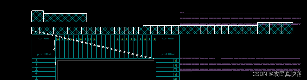
如图所示,我们将红框内放大,可以看到pad的具体名称。


其中test_mode_iopad在最上面,是order最大的,即对应命令
set_pad_physical_constraints -pad_name "test_mode_iopad" -side 3 -order 22
可以得出结论,order的顺序是左下角最小,从左往后以此增大,从上往下依次增大,即坐标轴的递增关系。
Initialize the floorplan:
Select Floorplan Initialize Floorplan…
Change the Core utilization to 0.8 (80%).
Change the Core to left/right/bottom/top spacing to 30.
Click OK.
这一段无需翻译
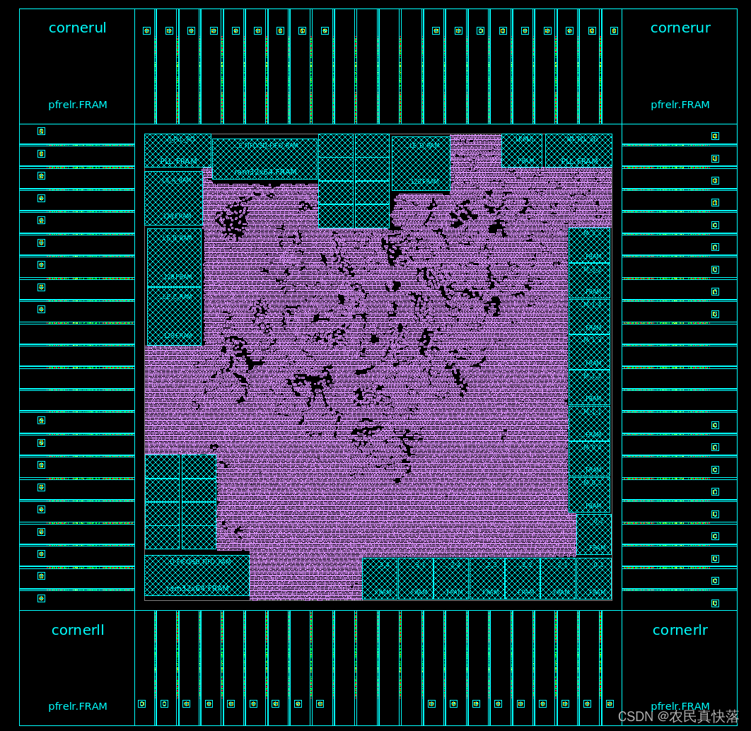
- Fit [F] the LayoutWindow and have a look at the chip’s core and periphery
areas. The blue hash-marked rectangles outside the chip along the top edge are
the unplaced macro cells. The purple objects along the right edge are all the
standard cells.
蓝色带散列标记的矩形是未布局的宏单元,右边缘紫色的是标准单元。
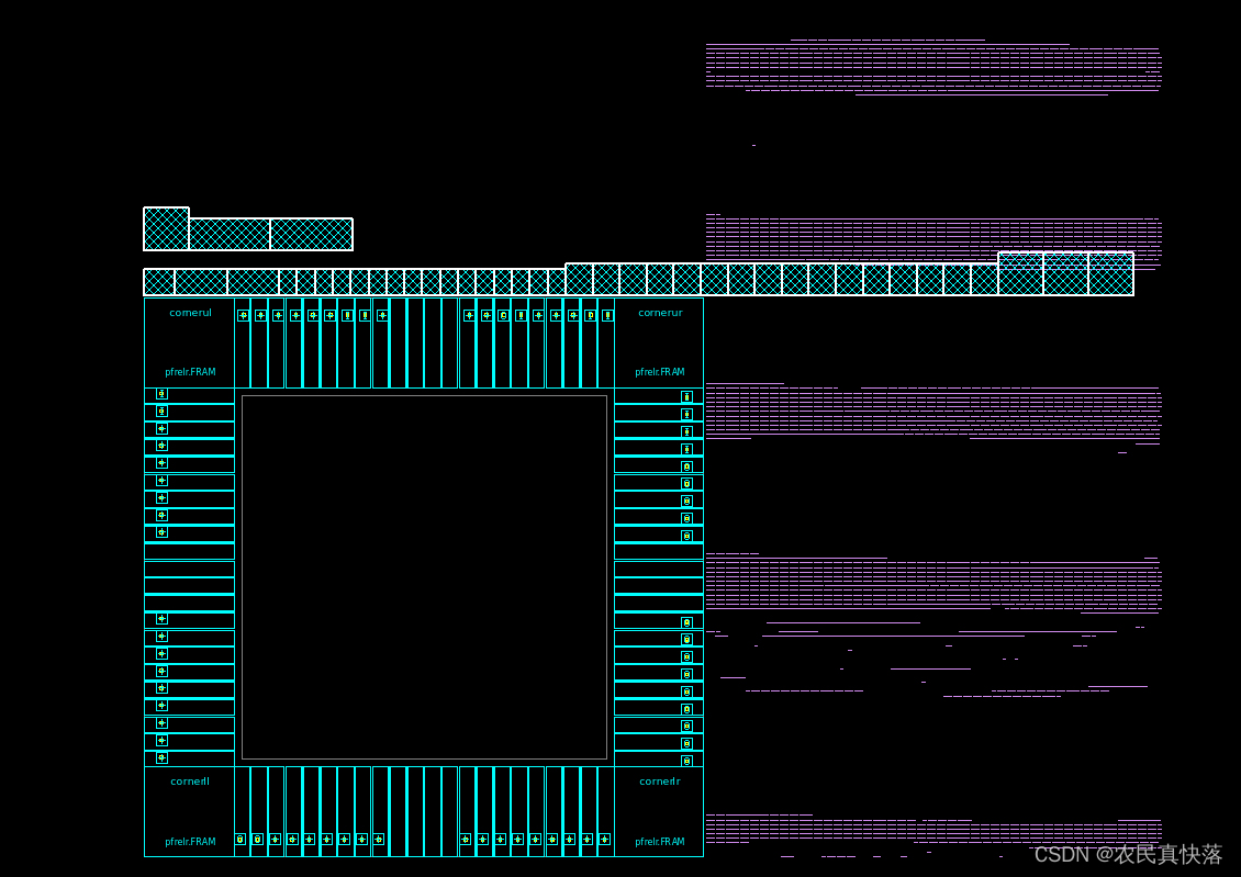
Note: The corner cells are easily visible – look at the large blue
square that takes up the full layout view (labeled pfrelr).
There are four groups of four P/G pads placed in the middle
of each side
注意:边角单元格很容易看到——看看占据整个布局视图的蓝色大方块(标记为pfrelr)。
有四组四个P/G放置在每边的中间。
个人总结:
图中蓝色的是macro cell,紫色的是std cell,图中的macro cell有3类,一类是corner cell,在四个角,一类是iopad,占据大部分,最后是vdd和vss,用作供电和接地。我现在认为这里的pad其实只是个框,方便后面布局放入真正的元件,目前并没有物理上的实际功能。
-
Zoom into the periphery area of the chip and notice that the spacing between
all the pads is about equal
放大到芯片的外围区域,注意到所有pad之间的间距大约相等 -
Insert the pad fillers to fill the gaps between the pads.
插入pad fillers来填补pad之间的gap
Depending on the technology and library being used, this may be needed for N- or P-well and/or for power/ground pad ring continuity.
根据所使用的技术和库,这可能需要用于P/N well或P/G pad ring continuity。
To keep the number of pad filler cells required to a minimum, specify the larger filler cells first in the list.
要将所需的填充单元格数量保持在最小值,先在列表中指定较大的filler单元。
Otherwise,a 1,000 um space will get filled with 200 x 5 um width cells, instead of one 1,000 um width cell. Enter the command in the box below or source the provided script scripts/insert_pad_filler.tcl
否则,一个1000um的空间将被200个5um的单元填满,而不是1个1000um宽度的单元。在下方的方框中输入命令,或者使用提供的脚本
scripts/insert_pad_filler.tcl
insert_pad_filler –cell "pfeed10000 pfeed05000 \
pfeed02000 pfeed01000 pfeed00500 pfeed00200 \
pfeed00100 pfeed00050 pfeed00010 pfeed00005"
man insert_pad_filler的部分结果:
ARGUMENTS
-cell lib_cells
Specifies the names of the pad filler cells to be used. The
tool adds the cells in the priority that they are specified.
也就是说,字符串中的序列就是优先级顺序,尽可能用大的filler,以减少填充的filler数量。
-
Zoom into the space between two pad cells and notice the filler cells that have
been inserted.
放大两个pad cell之间的空间,注意到filler cell已经被插入了。

-
Make the “logical” connection (no physical routing) between the
power/ground signals and all power/ground pins of the I/O pads, macros and
standard cells, by executing the following script:
通过执行以下脚本,在P/G信号和I/O pad,macro和std cell之间建立逻辑连接
source –echo scripts/connect_pg.tcl
Note: There are 3 different power supplies in this design: VDD,
VDDQ and VDDO. The latter two are used in the periphery
of the chip.
**注意:**本设计有3种不同的电源VDD VDDQ VDDO,后两个用在芯片的外围。
- Build the PAD area power supply ring: create_pad_rings
创建PAD区域电源环:create_pad_rings
Zoom into the area between the pads to see that metal routes have been added, over the filler cells, to connect the existing power routes within each pad cell to form continuous P/G pad rings.
放大PAD之间的区域,可以看到在填充单元上已经添加了金属线路,以连接每个PAD单元内现有的电源路由,形成连续的P/G PAD环。
- Save the design as “floorplan_init”:
save_mw_cel –as floorplan_init
2.3 Preplace the Macros Connected to I/O Pads
In this task you will identify the macros that are connected to I/O pad cells and you
will manually place them in the core area such that their connections to the I/O pads
are as short as possible.
在本任务中,您将识别连接到I/O pad单元的宏,并将它们手动放置在核心区域中,以便它们与I/O pad的连接尽可能短。
-
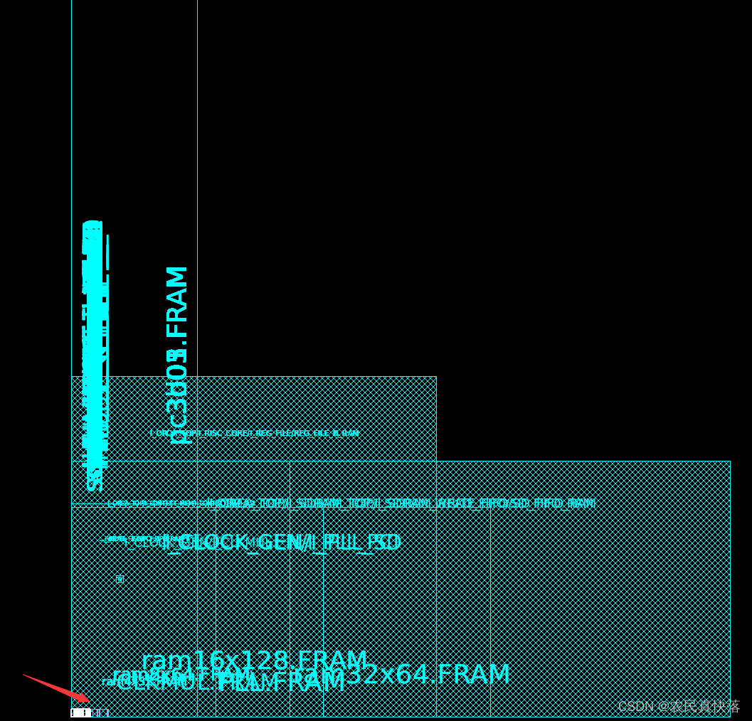
Zoom in to see the top periphery area shown in Figure 1 below.
放大去看顶层的边缘区域,如下图1所示 -
Identify macros that connect to I/O pads, as follows:
查看连接到I/O pad的宏,如下:
Choose Select -> Cells ->By Types…
选择Select->Cell->By Types
Click the Uncheck All button in the top (Cell Type) section of the dialog box.
点击对话框中顶部的Uncheck All 按钮
Select the Macro cell type check box.
选择Macro cell种类的勾选框
Click the Select All button in lower left corner of the dialog box.
点击Select All按钮在对话框的左下角
Click OK.
点击OK
Notice that all the macros are now selected – highlighted in white.
注意所有macro现在都被选中了,以白色高亮。
Select the Flylines button from the top banner section of the LayoutWindow.
从LayoutWindow的顶部选择Flylines按钮
In the “Show flylines” panel that appears on the right side of the window click on the pull-down menu and choose Select to IO and Apply.
在窗口右侧的Show flylines面板中点击下拉菜单并选中Select to IO并Apply
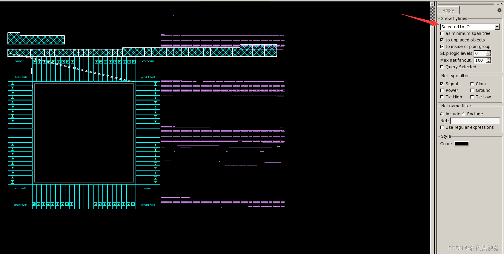
Reduce the “brightness” to 50% or less to better see the three flylines.The three lower left macros show connections to the top IO pads.
把"亮度"调整到50%或者更小,以更好地看见3条飞线。左下角的三个macro显示了到顶层IO端口的连线。
- Keep the “Show flylines” panel open and,if needed,adjust the viewing area(pan/zoom) to see the picture below.If you accidentally unselect the macros and the flylines disappear,use the [Ctrl] key to reselect the three circled macros shown here,and the flylines will reappear.
保持"Show flylines"面板打开,并且如果需要的话调整视图区域以查看下面的图。如果你意外地失去选中这些宏并飞线消失了,使用[Ctrl]键去重新选中这三个macros,并且飞线会重新出现。
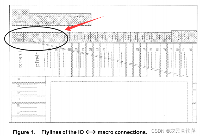
- The three macros with a direct connection to IO pad cells are called I_CLOCK_GEN/I_PLL_PCI, I_CLOCK_GEM_PLL_SD and I_CLOCK_GEN/I_CLKMUL. Hover your mouse arrow over a cell to see its
information window in the lower-left area. The two PLLs in this design should
be placed towards the top left and right corners of the chip so they are closer
to their respective clock pads.
这三个与IO pad 单元有直接连接的宏分别是
I_CLOCK_GEN/I_PLL_PCI
I_CLOCK_GEM_PLL_SD
I_CLOCK_GEN/I_CLKMUL
将你的鼠标箭头悬浮在一个cell上可以在左下角区域查看到它的信息。在该设计中这两个PLL应当被放置在芯片的左上方和右上方,这样他们会比较靠近响应的时钟pad。
- Now you will manually move the I_PLL_PCI macro,which is connected to the left pad,into the core area.Keep in mind that you can use the undo button to back track your steps.
现在你将手动移动这个和左边pad有连接的I_PLL_PCI宏,移动到core area.记住你可以使用undo按钮(Ctrl + z)去回退你的步骤。
a. Select just the I_PLL_PCI macro using Selection Tool button.
只选择I_PLL_PCI宏用Selection 工具按钮(就是正常的箭头)
b. Select the Move/Resize Tool (M) I® button (may be in the left banner of the window) to begin the moving process.
选择移动按钮(按M),在窗口左侧选项栏,来开始移动的过程。
Drag the I_PLL_PCI macro to approximately the top-left comer of the core area. Leave some room to the edges of the core.
拖动I_PLL_PCI 宏到核心区域大概左上角的位置。注意离core的边界一点空间。
c. With the PLL still selected, use the align functions to align the PLL to the top and left edges o f the core:
Click the Align Objects to Left align it to the core’s left edge button to From the pull-down menu select the Align Objects’
to Top button to align it to the core’s top edge
The PLL is now aligned with the edges of the core.
保持PLL仍然被选中,使用对其功能去对其PLL到core的上面和左边的边缘:
点击Align Objects to left按钮将其对其到核心左侧边缘,从下拉菜单中选择Align Objects to Top按钮来将它对齐到core的顶部边缘。
这个PLL现在对齐到了core的边缘。
d.To make sure that the cell is not moved by virtual flat placement, click on the “padlock button to lock it down. You should see an X through the cell now.
为了保证cell不被virtual flat placement移动,点击padlock按钮去把它锁起来。(也在窗口左侧工具栏)
This is an alternative to using set_dont_touch_placement.
-
Try to move the “fixed” I_PLL_PCI macro.You should not be able to do so.If you are able to move it,use the undo button to put it back and “fix” it in place. Don’t worry if you make a mistake since you will be provided with a script to place these macros at the expected coordinates in a later step.
Use the ESC key as needed to return the cursor to the “select” mode.
尝试去移动这个“fixed”I_PLL_PCI 宏。你会发现现在做不到了。如果你能移动的话,使用undo按钮来撤回并修正到正确的位置。别担心你会犯错因为你稍后会提供一个脚本来放置这些宏到预期的坐标。
使用ESC键来使光标回到“选择”模式。 -
In the next steps you will repeat the steps above to move the other two macros
into the core area and near their respective IO pad cells. DO NOT spend too
much time on this step to get them perfectly placed. A script in the next step
will ensure correct placement
下面的步骤中你会重复这些上述的步骤来移动另外两个macro到核心区域并且靠近他们对应的IO端口单元。不要花太多时间在这一步来得到他们完美的位置。下一步会给个脚本来确保正确地布局。

点击I_PLL_SD来选择它,移动到core区域的右上角并对齐到右边和上边的边上。将其旋转180°以减少其互联线的长度。点击padlock按钮来锁住它。
选择并拖动I_CLKMUL到I_PLL_SD的左边。对齐到顶部的边。
从窗口左侧工具栏中的"Rotate"下拉菜单中选择Y-axis来沿Y方向镜像(=在x方向翻转)以减少线长。
将I_CLKMUL和I_PLL_SD空出10个microns,使用Ctrl键选中这两个macro,指定分离偏置为10.
选择分离对象到右边按钮,再看I_CLKMUL 宏
点击小×关闭右侧的飞线面板。
你应当在选中宏时能看到一个大×。剩下的宏和标准单元将在下面的VF布局步骤中被放置好。
- 为了保证三个宏能放置好,可以source如下脚本
source -echo scripts/preplace_macros.tcl
2.4 Perform Virtual Flat Placement
Normally, prior to performing virtual flat placement, any known macro placement constraints as well as hard/soft placement blockages should be defined. We will skip these steps initially so that you can observe the “default” VF placement
behavior. After the first placement the above constraint will be applied and VF
placement will be performed again. You will notice a marked difference.
通常,在执行VFP之前,任何已知的宏放置约束以及硬/软布局块该被定义。
我们一开始将跳过这些步骤,以便观察“默认”VFP行为。在第一次布局后上面的约束将被应用并且VFP将再次被执行。
您将注意到一个显著的差异。
- Verify that the current VF placement strategy options have default settings:
验证当前的VFP策略选项由默认的设置
report_fp_placement_strategy
- Apply a sliver size of 10 to prevent standard cells from being placed in narrow channels(<10um)between macros:
为防止标准单元被放置在小于10um的狭窄通道中,应用大小为10um的条带
set_fp_placement_strategy -sliver_size 10
- Execute a timing-driven VF placement with “no hierarchy gravity”(to ensure that the “logical hierarchy” does not affect placement of this non-hierarchical or flat layout):
在“无层级重力”的情况下执行一个时间驱动的VF版图(以确保“逻辑层级”不会影响这个无层级或扁平布局的版图):
create_fp_placement -timing_driven -no_hierarchy_gravity
- Examine the global route congestion map:

检查全局路径拥塞图
点击全局路径拥塞图按钮,在弹出的面板上点击reload按钮
弹出了一个对话框,包含下面这条待执行的的阻塞分析命令。
点击OK
- An “Errors” box appears in the GUI - click OK.
If you scroll up in the log to the beginning of the congestion analysis output, you will see an “Error” message (PSYN-348) about a macro that “is not fixed”. You can safely ignore this. You could “fix” all macro placements prior to the congestion analysis to avoid the PSYN-348 error. However, you will be running create_fp_placement again to modify macro placement, so you don’t want fixed placement on the macros yet.
一个“错误”框出现在GUI中,点击确定。如果您向上滚动日志到拥塞分析输出的开始,您将看到一个关于宏的“错误”消息(PSYN-348) 是"is not fixed"。你可以放心地忽略它。你可以在拥塞分析之前“fix”所有宏布局以避免出现psyn -348错误。但是,你可以再次运行create_fp_placement来修改宏布局,所以你目前还不希望宏的位置固定。
-
Close the Global Route Congestion panel on the right by clicking on the small “x” in its upper right corner.
关闭右侧的Global Route Congestion面板通过点右上角的小× -
Routing of power and ground straps and macro rings for this design can be made easier if we turn some of the macros into arrays.Source the script below to apply macro placement constraints to accomplish the following goals.
如果我们将一些macro放到array中,布线该设计的电源和接地straps和macro环会更容易。Source这个脚本以应用macro布局约束来完成下面的目标。
- Place macros as close to the edges of the chip as possible
尽可能贴近芯片地布局宏 - Group macros together as much as possible
尽可能将宏放在一起 - Turn on virtual IPO to mimic timing optimization (and prevent
unnecessary placement optimization)
打开虚拟IPO以模拟定时优化(并防止不必要的布局优化) - Limit the legal placement orientation of some RAMs
限制一些RAM的合法布局方向
source -echo scripts/macro_place_cons.tcl
- Double check your settings.Suggestions:Use the up-arrow in the icc_shell window to find and re-execute the “strategy” command:
二次检查你的设置。建议:使用icc窗口中的向上箭头去找到并重新执行strategy命令:
report_fp_placement_strategy
report_fp_macro_options
- Source the following script to set a hard keepout margin of 10 microns around all macros. This will make it easier to create P/G rings around the macros and avoid congestion as well as signal routing DRCs around the macros:
参考下面的脚本在所有的宏周围设置一个10微米左右的硬边界。这将使得在宏周围创建P/G环更加容易,并避免拥塞以及围绕宏的信号路由DRC:
source -echo scripts/keepout.tcl
- Take one last look at the macro placement before running the VF placer again:
在再次运行VF placer之前再次看一遍宏布局
create_fp_placement -timing_driven -no_hierarchy_gravity
-
Analyze the global route congestion map again. You need to click Reload OK to update the map. An “Error” box appears in the GUI - click OK (similar to step5).
There should not be any congestion issues.
Close the analysis panel on the right by clicking on the small “x”.
再次分析全局布线阻塞图。分析完以后关闭该面板。 -
Lock down all macros:
set_dont_touch_placement [all_macro_cells] -
Save the cell:
save_mw_cel -as floorplan_placed


 422
422


 被折叠的 条评论
为什么被折叠?
被折叠的 条评论
为什么被折叠?
 到【灌水乐园】发言


