


FPGA学习RAM单端口练习
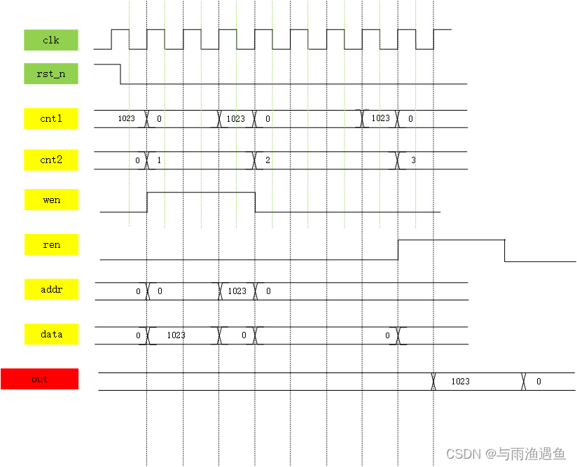
时序图
ram.v
module ram (
    input wire clk,
    input wire rst_n,
    output wire [9:0]rddata
);

reg [9:0]cnt1;
reg [1:0]cnt2;
reg [9:0]data;
reg [9:0]addr;
reg ren;
reg wen;

always @(posedge clk or negedge rst_n) begin
    if (~rst_n) begin
        cnt1 <= 10'd0;
    end
    else if (cnt1 == 10'd1023) begin
        cnt1 <= 10'd0;
    end
    else begin
        cnt1 <= cnt1 + 10'd1;
    end
end

always @(posedge clk or negedge rst_n) begin
    if (~rst_n) begin
        cnt2 <= 2'd0;
    end
    else if (cnt2 == 3'd3 && cnt1 == 10'd1023) begin
        cnt2 <= 2'd0;
    end
    else if (cnt1 == 10'd1023) begin
        cnt2 <= cnt2 + 10'd1;
    end
    else begin
        cnt2 <= cnt2;
    end
end

always @(posedge clk or negedge rst_n) begin
    if (~rst_n) begin
        wen <= 1'b0;
    end
    else if (cnt2 == 2'd0 && cnt1 == 10'd1023) begin
        wen <= ~wen;
    end
    else if (cnt2 == 2'd1 && cnt1 == 10'd1023) begin
        wen <= ~wen;
    end
    else begin
        wen <= wen;
    end
end

always @(posedge clk or negedge rst_n) begin
    if (~rst_n) begin
        ren <= 1'b0;
    end
    else if (cnt2 == 2'd2 && cnt1 == 10'd1023) begin
        ren <= ~ren;
    end
     else if (cnt2 == 2'd3 && cnt1 == 10'd1023) begin
        ren <= ~ren;
    end
    else begin
        ren <= ren;
    end
end

always @(posedge clk or negedge rst_n) begin
    if (~rst_n) begin
        addr <= 10'd0;
    end
    else if (cnt1 == 10'd1023) begin
        addr <= 10'd0;
    end
    else begin
        addr <= addr + 10'd1;
    end
end


always @(posedge clk or negedge rst_n) begin
    if (~rst_n) begin
        data <= 10'd0;
    end
    else if (cnt1 == 10'd1023) begin
        data <= 10'd1023;
    end
    else begin
        data <= data - 10'd1;
    end
end


ip_ram	ip_ram_inst (
	.address ( addr ),
	.clock ( clk ),
	.data ( data),
	.rden ( ren ),
	.wren ( wen ),
	.q ( rddata )
);

endmodule
ram_tb.v
`timescale 1ns/1ps

module ram_tb ();


reg clk;
reg rst_n;
wire [9:0]rddata;

initial begin
    clk = 1'b0;
    rst_n = 1'b0;
    #2
    rst_n = 1'b1;
end

always #10 clk = ~clk;

ram ram_1 (
    .clk(clk),
    .rst_n(rst_n),
    .rddata(rddata)
);

endmodule
仿真
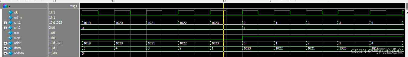
写数据
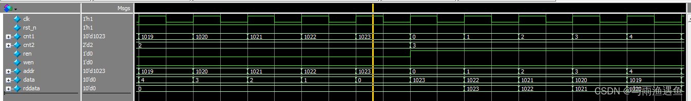
 读数据
读数据
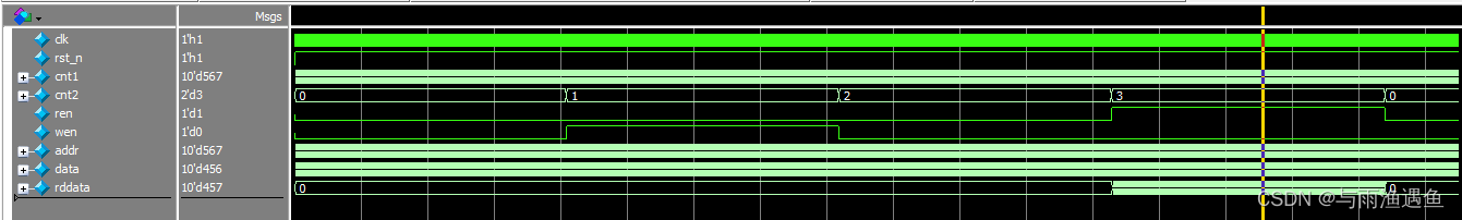
 整体
整体


 4734
4734


 被折叠的 条评论
为什么被折叠?
被折叠的 条评论
为什么被折叠?
 到【灌水乐园】发言


