


声明:原文版权归属Intel®,这里仅作学习使用
来源:Intel® 64 and IA-32 Architectures Software Developer's Manual Volume 3A: System Programming Guide, Part 1
Chapter 2.6 SYSTEM INSTRUCTION SUMMARY 系统指令总结
System instructions handle system-level functions such as loading system registers, managing the cache, managing interrupts, or setting up the debug registers. Many of these instructions can be executed only by operating-system or executive procedures (that is, procedures running at privilege level 0)(其中许多指令只能在特权级0下执行). Others can be executed at any privilege level and are thus available to application programs.
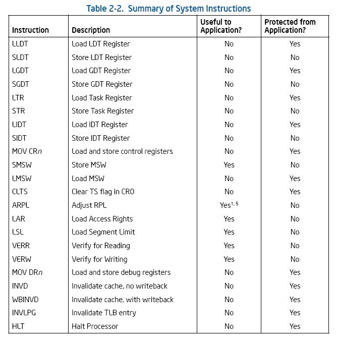
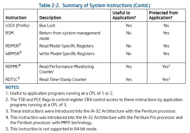
Table 2-2 lists the system instructions and indicates whether they are available and useful for application programs. These instructions are described in the Intel® 64 and IA-32 Architectures Software Developer’s Manual, Volumes 2A & 2B.
2.6.1 Loading and Storing System Registers
The GDTR, LDTR, IDTR, and TR registers each have a load and store instruction for loading data into and storing data from the register:
•LGDT (Load GDTR Register) — Loads the GDT base address and limit from memory into the GDTR register.
•SGDT (Store GDTR Register) — Stores the GDT base address and limit from the GDTR register into memory.
•LIDT (Load IDTR Register) — Loads the IDT base address and limit from memory into the IDTR register.
•SIDT (Load IDTR Register) — Stores the IDT base address and limit from the IDTR register into memory.
•LLDT (Load LDT Register) — Loads the LDT segment selector and segment descriptor from memory into the LDTR. (The segment selector operand can also be located in a general-purpose register.)
•SLDT (Store LDT Register) — Stores the LDT segment selector from the LDTR register into memory or a general-purpose register.
•LTR (Load Task Register) — Loads segment selector and segment descriptor for a TSS from memory into the task register. (The segment selector operand can also be located in a general-purpose register.)
•STR (Store Task Register) — Stores the segment selector for the current task TSS from the task register into memory or a general-purpose register.
The LMSW (load machine status word) and SMSW (store machine status word) instructions operate on bits 0 through 15 of control register CR0. These instructions are provided for compatibility with the 16-bit Intel 286 processor. Programs written to run on 32-bit IA-32 processors should not use these instructions. Instead, they should access the control register CR0 using the MOV instruction.
The CLTS (clear TS flag in CR0) instruction is provided for use in handling a device-not-available exception (#NM) that occurs when the processor attempts to execute a floating-point instruction when the TS flag is set. This instruction allows the TS flag to be cleared after the x87 FPU context has been saved, preventing further #NM exceptions. See Section 2.5, “Control Registers,” for more information on the TS flag.
The control registers (CR0, CR1, CR2, CR3, CR4, and CR8) are loaded using the MOV instruction. The instruction loads a control register from a general-purpose register or stores the content of a control register in a general-purpose register.
2.6.2 Verifying of Access Privileges
The processor provides several instructions for examining segment selectors and segment descriptors to determine if access to their associated segments is allowed. These instructions duplicate some of the automatic access rights and type checking done by the processor, thus allowing operating-system or executive software to prevent exceptions from being generated.
The ARPL (adjust RPL) instruction adjusts the RPL (requestor privilege level) of a segment selector to match that of the program or procedure that supplied the segment selector. See Section 4.10.4, “Checking Caller Access Privileges (ARPL Instruction),” for a detailed explanation of the function and use of this instruction. Note that ARPL is not supported in 64-bit mode.
The LAR (load access rights) instruction verifies the accessibility of a specified segment and loads access rights information from the segment’s segment descriptor into a general-purpose register. Software can then examine the access rights to determine if the segment type is compatible with its intended use. See Section 4.10.1, “Checking Access Rights (LAR Instruction),” for a detailed explanation of the function and use of this instruction.
The LSL (load segment limit) instruction verifies the accessibility of a specified segment and loads the segment limit from the segment’s segment descriptor into a general-purpose register. Software can then compare the segment limit with an offset into the segment to determine whether the offset lies within the segment. See Section 4.10.3, “Checking That the Pointer Offset Is Within Limits (LSL Instruction),” for a detailed explanation of the function and use of this instruction.
The VERR (verify for reading) and VERW (verify for writing) instructions verify if a selected segment is readable or writable, respectively, at a given CPL. See Section 4.10.2, “Checking Read/Write Rights (VERR and VERW Instructions),” for a detailed explanation of the function and use of this instruction.
2.6.3 Loading and Storing Debug Registers
Internal debugging facilities in the processor are controlled by a set of 8 debug registers (DR0-DR7). The MOV instruction allows setup data to be loaded to and stored from these registers.
On processors that support Intel 64 architecture, debug registers DR0-DR7 are 64 bits. In 32-bit modes and compatibility mode, writes to a debug register fill the upper 32 bits with zeros. Reads return the lower 32 bits. In 64-bit mode, the upper 32 bits of DR6-DR7 are reserved and must be written with zeros. Writing one to any of the upper 32 bits causes an exception, #GP(0).
In 64-bit mode, MOV DRn instructions read or write all 64 bits of a debug register (operand-size prefixes are ignored). All 64 bits of DR0-DR3 are writable by software. However, MOV DRn instructions do not check that addresses written to DR0-DR3 are in the limits of the implementation. Address matching is supported only on valid addresses generated by the processor implementation.
2.6.4 Invalidating Caches and TLBs
The processor provides several instructions for use in explicitly invalidating its caches and TLB entries. The INVD (invalidate cache with no writeback) instruction invalidates all data and instruction entries in the internal caches and sends a signal to the external caches indicating that they should be also be invalidated.
The WBINVD (invalidate cache with writeback) instruction performs the same function as the INVD instruction, except that it writes back modified lines in its internal caches to memory before it invalidates the caches. After invalidating the internal caches, WBINVD signals external caches to write back modified data and invalidate their contents.
The INVLPG (invalidate TLB entry) instruction invalidates (flushes) the TLB entry for a specified page.
2.6.5 Controlling the Processor
The HLT (halt processor) instruction stops the processor until an enabled interrupt (such as NMI or SMI, which are normally enabled), a debug exception, the BINIT# signal, the INIT# signal, or the RESET# signal is received. The processor generates a special bus cycle to indicate that the halt mode has been entered.
Hardware may respond to this signal in a number of ways. An indicator light on the front panel may be turned on. An NMI interrupt for recording diagnostic information may be generated. Reset initialization may be invoked (note that the BINIT# pin was introduced with the Pentium Pro processor). If any non-wake events are pending during shutdown, they will be handled after the wake event from shutdown is processed (for example, A20M# interrupts).
The LOCK prefix invokes a locked (atomic) read-modify-write operation(上锁(原子的)读写操作) when modifying a memory operand. This mechanism is used to allow reliable communications between processors in multiprocessor systems, as described below:
•In the Pentium processor and earlier IA-32 processors, the LOCK prefix causes the processor to assert the LOCK# signal during the instruction. This always causes an explicit bus lock to occur.
•In the Pentium 4, Intel Xeon, and P6 family processors, the locking operation is handled with either a cache lock or bus lock. If a memory access is cacheable and affects only a single cache line, a cache lock is invoked and the system bus and the actual memory location in system memory are not locked during the operation. Here, other Pentium 4, Intel Xeon, or P6 family processors on the bus write-back any modified data and invalidate their caches as necessary to maintain system memory coherency. If the memory access is not cacheable and/or it crosses a cache line boundary, the processor’s LOCK# signal is asserted and the processor does not respond to requests for bus control during the locked operation.
The RSM (return from SMM) instruction restores the processor (from a context dump) to the state it was in prior to an system management mode (SMM) interrupt.
2.6.6 Reading Performance-Monitoring and Time-Stamp Counters
The RDPMC (read performance-monitoring counter) and RDTSC (read time-stamp counter) instructions allow application programs to read the processor’s performance-monitoring and time-stamp counters, respectively. Pentium 4 and Intel Xeon processors have eighteen 40-bit performance-monitoring counters; P6 family processors have two 40-bit counters.
Use these counters to record either the occurrence or duration of events.(用计数器记录事件发生的次数或者持续时间) Events that can be monitored are model specific; they may include the number of instructions decoded, interrupts received, or the number of cache loads. Individual counters can be set up to monitor different events. Use the system instruction WRMSR to set up values in the one of the 45 ESCRs and one of the 18 CCCR MSRs (for Pentium 4 and Intel Xeon processors); or in the PerfEvtSel0 or the PerfEvtSel1 MSR (for the P6 family processors). The RDPMC instruction loads the current count from the selected counter into the EDX:EAX registers.
The time-stamp counter is a model-specific 64-bit counter that is reset to zero each time the processor is reset. If not reset, the counter will increment ~9.5 x 10¹⁶ times per year when the processor is operating at a clock rate of 3GHz. At this clock frequency, it would take over 190 years for the counter to wrap around. The RDTSC instruction loads the current count of the time-stamp counter into the EDX:EAX registers.
See Section 18.11, “Performance Monitoring Overview,” and Section 18.10, “Time-Stamp Counter,” for more information about the performance monitoring and time-stamp counters.
The RDTSC instruction was introduced into the IA-32 architecture with the Pentium processor. The RDPMC instruction was introduced into the IA-32 architecture with the Pentium Pro processor and the Pentium processor with MMX technology. Earlier Pentium processors have two performance-monitoring counters, but they can be read only with the RDMSR instruction, and only at privilege level 0.
2.6.7 Reading and Writing Model-Specific Registers
The RDMSR (read model-specific register) and WRMSR (write model-specific register) instructions allow a processor’s 64-bit model-specific registers (MSRs) to be read and written, respectively. The MSR to be read or written is specified by the value in the ECX register.
RDMSR reads the value from the specified MSR to the EDX:EAX registers; WRMSR writes the value in the EDX:EAX registers to the specified MSR. RDMSR and WRMSR were introduced into the IA-32 architecture with the Pentium processor.
See Section 9.4, “Model-Specific Registers (MSRs),” for more information.


 773
773


 被折叠的 条评论
为什么被折叠?
被折叠的 条评论
为什么被折叠?
 到【灌水乐园】发言


