


声明:原文版权归属Intel®,这里仅作学习使用
来源:Intel® 64 and IA-32 Architectures Software Developer's Manual Volume 3A: System Programming Guide, Part 1
Chapter 2.5 CONTROL REGISTERS 控制寄存器
Control registers (CR0, CR1, CR2, CR3, and CR4; see Figure 2-6) determine operating mode of the processor and the characteristics of the currently executing task. (控制寄存器决定了处理器的运行模式以及当前执行任务的特征)These registers are 32 bits in all 32-bit modes and compatibility mode.
In 64-bit mode, control registers are expanded to 64 bits. The MOV CRn instructions are used to manipulate the register bits. Operand-size prefixes for these instructions are ignored. The following is also true:
•Bits 63:32 of CR0 and CR4 are reserved(保留) and must be written with zeros. Writing a nonzero value to any of the upper 32 bits results in a general-protection exception, #GP(0).
•All 64 bits of CR2 are writable by software.
•Bits 51:40 of CR3 are reserved and must be 0.
•The MOV CRn instructions do not check that addresses written to CR2 and CR3 are within the linear-address or physical-address limitations of the implementation.
•Register CR8 is available in 64-bit mode only.
The control registers are summarized below, and each architecturally defined control field in these control registers are described individually. In Figure 2-6, the width of the register in 64-bit mode is indicated in parenthesis (except for CR0).
•CR0 — Contains system control flags that control operating mode and states of the processor.(包含控制运行模式和处理器状态的系统控制标志位)
•CR1 — Reserved.
•CR2 — Contains the page-fault linear address (the linear address that caused a page fault).(保存产生缺页错误的线性地址)
•CR3 — Contains the physical address of the base of the page directory and two flags (PCD and PWT). This register is also known as the page-directory base register (PDBR)(页目录基址寄存器). Only the most-significant bits (less the lower 12 bits) of the base address are specified; the lower 12 bits of the address(地址的低12位为0) are assumed to be 0. The page directory must thus be aligned to a page (4-KByte) boundary(与4K字节页对齐). The PCD and PWT flags control caching of the page directory in the processor’s internal data caches (they do not control TLB caching of page-directory information).
When using the physical address extension, the CR3 register contains the base address of the page-directory-pointer table In IA-32e mode, the CR3 register contains the base address of the PML4 table.
See also: Section 3.8, “36-Bit Physical Addressing Using the PAE Paging Mechanism.”(PAE下36位物理寻址的机制有别于普通情况)
•CR4 — Contains a group of flags that enable several architectural extensions, and indicate operating system or executive support for specific processor capabilities.The control registers can be read and loaded (or modified) using the move-to-or-from-control-registers forms of the MOV instruction. In protected mode, the MOV instructions allow the control registers to be read or loaded (at privilege level 0 only). This restriction means that application programs or operating-system procedures (running at privilege levels 1, 2, or 3) are prevented from reading or loading the control registers.
•CR8 — Provides read and write access to the Task Priority Register (TPR). It specifies the priority threshold value that operating systems use to control the priority class of external interrupts allowed to interrupt the processor. This register is available only in 64-bit mode. However, interrupt filtering continues to apply in compatibility mode.
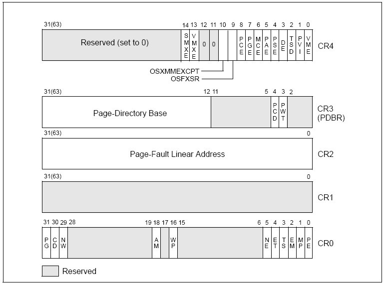
Figure 2-6. Control Registers
When loading a control register, reserved bits should always be set to the values previously read. The flags in control registers are:
下面是CR0控制寄存器的标志位:
PG Paging (bit 31 of CR0)(分页位) — Enables paging when set; disables paging when clear. When paging is disabled, all linear addresses are treated as physical addresses. The PG flag has no effect if the PE flag (bit 0 of register CR0) is not also set; setting the PG flag when the PE flag is clear causes a general-protection exception (#GP). See also: Section 3.6, “Paging (Virtual Memory) Overview.”
On Intel 64 processors, enabling and disabling IA-32e mode operation also requires modifying CR0.PG.
CD Cache Disable (bit 30 of CR0)(关缓存位) — When the CD and NW flags are clear, caching of memory locations for the whole of physical memory in the processor’s internal (and external) caches is enabled. When the CD flag is set, caching is restricted as described in Table 10-5. To prevent the processor from accessing and updating its caches, the CD flag must be set and the caches must be invalidated so that no cache hits can occur.
See also: Section 10.5.3, “Preventing Caching,” and Section 10.5, “Cache Control.”
NW Not Write-through (bit 29 of CR0)(非直写位) — When the NW and CD flags are clear, write-back (for Pentium 4, Intel Xeon, P6 family, and Pentium processors) or write-through (for Intel486 processors) is enabled for writes that hit the cache and invalidation cycles are enabled. See Table 10-5 for detailed information about the affect of the NW flag on caching for other settings of the CD and NW flags.
AM Alignment Mask (bit 18 of CR0)(对齐屏蔽位) — Enables automatic alignment checking when set; disables alignment checking when clear. Alignment checking is performed only when the AM flag is set, the AC flag in the EFLAGS register is set, CPL is 3, and the processor is operating in either protected or virtual-8086 mode.
WP Write Protect (bit 16 of CR0)(写保护位) — Inhibits supervisor-level procedures from writing into user-level read-only pages when set; allows supervisor-level procedures to write into user-level read-only pages when clear (regardless of the U/S bit setting; see Section 3.7.6). This flag facilitates implementation of the copy-on-write(写时拷贝) method of creating a new process (forking) used by operating systems such as UNIX.
NE Numeric Error (bit 5 of CR0)(数字错误位) — Enables the native (internal) mechanism for reporting x87 FPU errors when set; enables the PC-style x87 FPU error reporting mechanism when clear. When the NE flag is clear and the IGNNE# input is asserted, x87 FPU errors are ignored. When the NE flag is clear and the IGNNE# input is deasserted, an unmasked x87 FPU error causes the processor to assert the FERR# pin to generate an external interrupt and to stop instruction execution immediately before executing the next waiting floating-point instruction or WAIT/FWAIT instruction.
The FERR# pin is intended to drive an input to an external interrupt controller (the FERR# pin emulates the ERROR# pin of the Intel 287 and Intel 387 DX math coprocessors). The NE flag, IGNNE# pin, and FERR# pin are used with external logic to implement PC-style error reporting.
See also: “Software Exception Handling” in Chapter 8, “Programming with the x87 FPU,” and Appendix A, “Eflags Cross-Reference,” in the Intel® 64 and IA-32 Architectures Software Developer’s Manual, Volume 1.
ET Extension Type (bit 4 of CR0)(扩展类型位) — Reserved in the Pentium 4, Intel Xeon, P6 family, and Pentium processors. In the Pentium 4, Intel Xeon, and P6 family processors, this flag is hardcoded to 1. In the Intel386 and Intel486 processors,
this flag indicates support of Intel 387 DX math coprocessor instructions(协处理器指令) when set.
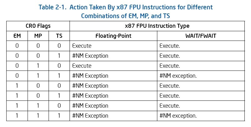
TS Task Switched (bit 3 of CR0)(任务切换位) — Allows the saving of the x87 FPU/MMX/SSE/SSE2/SSE3/SSSE3/SSE4 context on a task switch to be delayed until an x87 FPU/MMX/SSE/SSE2/SSE3/SSSE3/SSE4 instruction is actually executed by the new task. The processor sets this flag on every task switch and tests it when executing x87 FPU/MMX/SSE/SSE2/SSE3/SSSE3/SSE4 instructions.
•If the TS flag is set and the EM flag (bit 2 of CR0) is clear, a device-not-available exception (#NM) is raised prior to the execution of any x87 FPU/MMX/SSE/ SSE2/SSE3/SSSE3/SSE4 instruction; with the exception of PAUSE, PREFETCHh, SFENCE, LFENCE, MFENCE, MOVNTI, CLFLUSH, CRC32, and POPCNT. See the paragraph below for the special case of the WAIT/FWAIT instructions.
•If the TS flag is set and the MP flag (bit 1 of CR0) and EM flag are clear, an #NM exception is not raised prior to the execution of an x87 FPU WAIT/FWAIT instruction.
•If the EM flag is set, the setting of the TS flag has no affect on the execution of x87 FPU/MMX/SSE/SSE2/SSE3/SSSE3/SSE4 instructions.
Table 2-1 shows the actions taken when the processor encounters an x87 FPU instruction based on the settings of the TS, EM, and MP flags. Table 11-1 and 12-1 show the actions taken when the processor encounters an MMX/SSE/SSE2/SSE3/SSSE3/SSE4 instruction.
The processor does not automatically save the context of the x87 FPU, XMM, and MXCSR registers on a task switch. Instead, it sets the TS flag, which causes the processor to raise an #NM exception whenever it encounters an x87 FPU/MMX/SSE /SSE2/SSE3/SSSE3/SSE4 instruction in the instruction stream for the new task (with the exception of the instructions listed above).
The fault handler for the #NM exception can then be used to clear the TS flag (with the CLTS instruction) and save the context of the x87 FPU, XMM, and MXCSR registers. If the task never encounters an x87 FPU/MMX/SSE/SSE2/SSE3//SSSE3/SSE4 instruction; the x87 FPU/MMX/SSE/SSE2/ SSE3/SSSE3/SSE4 context is never saved.
EM Emulation (bit 2 of CR0)(仿真位) — Indicates that the processor does not have an internal or external x87 FPU when set; indicates an x87 FPU is present when clear. This flag also affects the execution of MMX/SSE/SSE2/SSE3/SSSE3/SSE4 instructions.
When the EM flag is set, execution of an x87 FPU instruction generates a device-not-available exception (#NM). This flag must be set when the processor does not have an internal x87 FPU or is not connected to an external math coprocessor. Setting this flag forces all floating-point instructions to be handled by software emulation. Table 9-2 shows the recommended setting of this flag, depending on the IA-32 processor and x87 FPU or math coprocessor present in the system. Table 2-1 shows the interaction of the EM, MP, and TS flags.
Also, when the EM flag is set, execution of an MMX instruction causes an invalid-opcode exception (#UD) to be generated (see Table 11-1). Thus, if an IA-32 or Intel 64 processor incorporates MMX technology, the EM flag must be set to 0 to enable execution of MMX instructions.
Similarly for SSE/SSE2/SSE3/SSSE3/SSE4 extensions, when the EM flag is set, execution of most SSE/SSE2/SSE3/SSSE3/SSE4 instructions causes an invalid opcode exception (#UD) to be generated (see Table 12-1). If an IA-32 or Intel 64 processor incorporates the SSE/SSE2/SSE3/SSSE3/SSE4 extensions, the EM flag must be set to 0 to enable execution of these extensions. SSE/SSE2/SSE3/SSSE3/SSE4 instructions not affected by the EM flag include: PAUSE, PREFETCHh, SFENCE, LFENCE, MFENCE, MOVNTI, CLFLUSH, CRC32, and POPCNT.
MP Monitor Coprocessor (bit 1 of CR0)(监控协处理器位). — Controls the interaction of the WAIT (or FWAIT) instruction with the TS flag (bit 3 of CR0). If the MP flag is set, a WAIT instruction generates a device-not-available exception (#NM) if the TS flag is also set. If the MP flag is clear, the WAIT instruction ignores the setting of the TS flag. Table 9-2 shows the recommended setting of this flag, depending on the IA-32 processor and x87 FPU or math coprocessor present in the system. Table 2-1 shows the interaction of the MP, EM, and TS flags.
PE Protection Enable (bit 0 of CR0)(保护使能位) — Enables protected mode when set; enables real-address mode when clear. This flag does not enable paging directly. It only enables segment-level protection. To enable paging, both the PE and PG flags must be set.(开启分页需要PE和PG标志同时设置)
See also: Section 9.9, “Mode Switching.”
下面是CR3控制寄存器的标志位:
PCD Page-level Cache Disable (bit 4 of CR3) — Controls caching of the current page directory. When the PCD flag is set, caching of the page-directory is prevented; when the flag is clear, the page-directory can be cached. This flag affects only the processor’s internal caches (both L1 and L2, when present). The processor ignores this flag if paging is not used (the PG flag in register CR0 is clear) or the CD (cache disable) flag in CR0 is set.
See also: Chapter 10, “Memory Cache Control” (for more about the use of the PCD flag) and Section 3.7.6, “Page-Directory and Page-Table Entries” (for a description of a companion PCD flag in page-directory and page-table entries).
PWT Page-level Writes Transparent (bit 3 of CR3) — Controls the write-through or write-back caching policy of the current page directory. When the PWT flag is set, write-through caching is enabled; when the flag is clear, write-back caching is enabled. This flag affects only internal caches (both L1 and L2, when present). The processor ignores this flag if paging is not used (the PG flag in register CR0 is clear) or the CD (cache disable) flag in CR0 is set.
See also: Section 10.5, “Cache Control” (for more information about the use of this flag), and Section 3.7.6, “Page-Directory and Page-Table Entries” (for a description of a companion PCD flag in the page-directory and page-table entries).
下面是CR4控制寄存器的标志位:
VME Virtual-8086 Mode Extensions (bit 0 of CR4) — Enables interrupt- and exception-handling extensions in virtual-8086 mode when set; disables the extensions when clear. Use of the virtual mode extensions can improve the performance of virtual-8086 applications by eliminating the overhead of calling the virtual-8086 monitor to handle interrupts and exceptions that occur while executing an 8086 program and, instead, redirecting the interrupts and exceptions back to the 8086 program’s handlers. It also provides hardware support for a virtual interrupt flag (VIF) to improve reliability of running 8086 programs in multitasking and multiple-processor environments.
See also: Section 15.3, “Interrupt and Exception Handling in Virtual-8086 Mode.”
PVI Protected-Mode Virtual Interrupts (bit 1 of CR4) — Enables hardware support for a virtual interrupt flag (VIF) in protected mode when set; disables the VIF flag in protected mode when clear. See also: Section 15.4, “Protected-Mode Virtual Interrupts.”
TSD Time Stamp Disable (bit 2 of CR4) — Restricts the execution of the RDTSC instruction to procedures running at privilege level 0 when set; allows RDTSC instruction to be executed at any privilege level when clear.
DE Debugging Extensions (bit 3 of CR4) — References to debug registers DR4 and DR5 cause an undefined opcode (#UD) exception to be generated when set; when clear, processor aliases references to registers DR4 and DR5 for compatibility with software written to run on earlier IA-32 processors.
See also: Section 18.2.2, “Debug Registers DR4 and DR5.”
PSE Page Size Extensions (bit 4 of CR4) — Enables large page sizes (2 or 4-MByte pages) when set; restricts pages to 4 KBytes when clear.
See also: Section 3.6.1, “Paging Options.”
PAE Physical Address Extension (bit 5 of CR4) — When set, enables paging mechanism to reference greater-or-equal-than-36-bit physical addresses. When clear, restricts physical addresses to 32 bits. PAE must be enabled to enable IA-32e mode operation. Enabling and disabling IA-32e mode operation also requires modifying CR4.PAE.
See also: Section 3.8, “36-Bit Physical Addressing Using the PAE Paging Mechanism.”
MCE Machine-Check Enable (bit 6 of CR4) — Enables the machine-check exception when set; disables the machine-check exception when clear.
See also: Chapter 14, “Machine-Check Architecture.”
PGE Page Global Enable (bit 7 of CR4) — (Introduced in the P6 family processors.)
Enables the global page feature when set; disables the global page feature when clear. The global page feature allows frequently used or shared pages to be marked as global to all users (done with the global flag, bit 8, in a page-directory or page-table entry). Global pages are not flushed from the translation-lookaside buffer (TLB) on a task switch or a write to register CR3.
When enabling the global page feature, paging must be enabled (by setting the PG flag in control register CR0) before the PGE flag is set. Reversing this sequence may affect program correctness, and processor performance will be impacted.
See also: Section 3.12, “Translation Lookaside Buffers (TLBs).”
PCE Performance-Monitoring Counter Enable (bit 8 of CR4) — Enables execution of the RDPMC instruction for programs or procedures running at any protection level when set; RDPMC instruction can be executed only at protection level 0 when clear.
OSFXSR
Operating System Support for FXSAVE and FXRSTOR instructions (bit 9 of CR4) — When set, this flag: (1) indicates to software that the operating system supports the use of the FXSAVE and FXRSTOR instructions, (2) enables the FXSAVE and FXRSTOR instructions to save and restore the contents of the XMM and MXCSR registers along with the contents of the x87 FPU and MMX registers, and (3) enables the processor to execute SSE/SSE2/SSE3/SSSE3/SSE4 instructions, with the exception of the PAUSE, PREFETCHh, SFENCE, LFENCE, MFENCE, MOVNTI, CLFLUSH, CRC32, and POPCNT.
If this flag is clear, the FXSAVE and FXRSTOR instructions will save and restore the contents of the x87 FPU and MMX instructions, but they may not save and restore the contents of the XMM and MXCSR registers. Also, the processor will generate an invalid opcode exception (#UD) if it attempts to execute any SSE/SSE2/SSE3and instruction, with the exception of PAUSE, PREFETCHh, SFENCE, LFENCE, MFENCE, MOVNTI, CLFLUSH, CRC32, and POPCNT. The operating system or executive must explicitly set this flag.
NOTE
CPUID feature flags FXSR indicates availability of the FXSAVE/FXRESTOR instructions. The OSFXSR bit provides operating system software with a means of enabling FXSAVE/FXRESTOR to save/restore the contents of the X87 FPU, XMM and MXCSR registers. Consequently OSFXSR bit indicates that the operating system provides context switch support for SSE/SSE2/SSE3/SSSE3/SSE4.
OSXMMEXCPT
Operating System Support for Unmasked SIMD Floating-Point Exceptions
(bit 10 of CR4) — When set, indicates that the operating system supports the handling of unmasked SIMD floating-point exceptions through an exception handler that is invoked when a SIMD floating-point exception (#XF) is generated. SIMD floating-point exceptions are only generated by SSE/SSE2/SSE3/SSE4.1 SIMD floating-point instructions.
The operating system or executive must explicitly set this flag. If this flag is not set, the processor will generate an invalid opcode exception (#UD) whenever it detects an unmasked SIMD floating-point exception.
VMXE
VMX-Enable Bit (bit 13 of CR4) — Enables VMX operation when set. See Chapter 19, “Introduction to Virtual-Machine Extensions.”
SMXE
SMX-Enable Bit (bit 14 of CR4) — Enables SMX operation when set. See Chapter 6, “Safer Mode Extensions Reference” of Intel® 64 and IA-32 Architectures Software Developer’s Manual, Volume 2B.
下面是CR8控制寄存器的标志位:
TPL Task Priority Level (bit 3:0 of CR8) — This sets the threshold value corresponding to the highest-priority interrupt to be blocked. A value of 0 means all interrupts are enabled. This field is available in 64-bit mode. A value of 15 means all interrupts will be disabled.
2.5.1 CPUID Qualification of Control Register Flags
The VME, PVI, TSD, DE, PSE, PAE, MCE, PGE, PCE, OSFXSR, and OSXMMEXCPT flags in control register CR4 are model specific(平台相关的). All of these flags (except the PCE flag) can be qualified with the CPUID instruction to determine if they are implemented on the processor before they are used.(使用CPUID指令判断处理器是否支持该功能)
The CR8 register is available on processors that support Intel 64 architecture.


 1940
1940

 被折叠的 条评论
为什么被折叠?
被折叠的 条评论
为什么被折叠?
 到【灌水乐园】发言


