


The same chart can be used for both impedance and admittance calculations. 常见形式的史密斯图,可以同时用于电感和导纳的计算
When the impedance form is used, this chart is a polar plot
of an S parameter. If the admittance form is used, the reflection coefficient is rotated 180 degree. 当使用电感形式,史密斯图即为散射系数
S
S
S的极坐标图。如果使用电导形式,反射系数需要旋转180°。
sample 01 确定传输线长度
Use a length of a terminated transmission line to realize an impedance of 140 j Ω j \Omega jΩ. 使用有端传输线的长度来实现140 j Ω j \Omega jΩ 的阻抗。
解:
First normalize impedance
140
j
Ω
/
Z
0
140j\Omega/Z_0
140jΩ/Z0
设
Z
0
=
100
Ω
Z_0=100\Omega
Z0=100Ω, normalize impedance=
1.4
j
1.4j
1.4j
140
j
Ω
j \Omega%
jΩ 纯虚数,纯导纳(total admittance),不消耗能量,所以传输线(TL)必须lossless——使传输线一端短路(short)或开路(open)可以实现。
1- 短路情况(short-circuit case)
在史密斯图中找到代表短路的点
A
A
A和代表
Z
0
=
1.4
j
Z_0=1.4j
Z0=1.4j的点B。

从外圈wavelengths toward generator刻度读出
A
,
B
A,B
A,B对应的长度,相减得传输线长度
l
A
=
0
λ
l
B
=
0.1515
λ
l
=
l
A
−
l
B
=
0.1515
λ
l_A=0\lambda \\ l_B=0.1515\lambda \\ l=l_A-l_B=0.1515\lambda
lA=0λlB=0.1515λl=lA−lB=0.1515λ
传输线长度在Smith Chart上表示为从
A
→
B
A \rightarrow B
A→B的路径(clockwise,即towards generator)

2- 开路情况(open-circuit case)
表示开路的点
A
′
A'
A′在外圆与“+x轴”交点处

l
A
‘
=
0.25
λ
l
B
=
0.1515
λ
l
=
l
A
’
+
l
B
=
0.4015
λ
(
c
l
o
c
k
w
i
s
e
,所以是相加)
l_A‘=0.25\lambda \\ l_B=0.1515\lambda \\ l=l_A’+l_B=0.4015\lambda(clockwise,所以是相加)
lA‘=0.25λlB=0.1515λl=lA’+lB=0.4015λ(clockwise,所以是相加)
sample 02 特殊电路情况的史密斯图表示
Special cases on Smith Chart.
-
阻抗匹配 Z = Z 0 Z=Z_0 Z=Z0

Normalized impedance=1, ∣ Γ ∣ = 0 |\Gamma|=0 ∣Γ∣=0, reactance x = 0 x=0 x=0, resistance r = 1 r=1 r=1, at the center.

-
电路中纯感抗 L L L
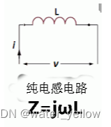
∣ Γ ∣ = 1 |\Gamma|=1 ∣Γ∣=1, reactance x > 0 x>0 x>0, resistance r = 0 r=0 r=0

沿最大圆( r = 0 r=0 r=0)的上半部分,随着频率 f f f增加逐渐向点 Γ r = 1 \Gamma_r=1 Γr=1靠近,即reactance x x x不断增大,频率达到无穷大相当于断路。 -
纯电容电路

Z = − j ω C Z=-\frac j {\omega C} Z=−ωCj, ∣ Γ ∣ = 1 |\Gamma|=1 ∣Γ∣=1, reactance x < 0 x<0 x<0, resistance r = 0 r=0 r=0

沿最大圆(
r
=
0
r=0
r=0)的下半部分,随着频率
f
f
f增加逐渐向点
Γ
r
=
−
1
\Gamma_r=-1
Γr=−1靠近,即reactance
x
x
x不断增大(负数增大即为靠近0),频率达到无穷大相当于短路。
- L C LC LC串联电路

Z
=
j
(
ω
L
−
1
ω
C
)
Z=j(\omega L-\frac 1 {\omega C})
Z=j(ωL−ωC1),
∣
Γ
∣
=
1
|\Gamma|=1
∣Γ∣=1, reactance
x
<
0
x<0
x<0, resistance
r
=
0
r=0
r=0

沿最大圆(
r
=
0
r=0
r=0)的顺时针方向,以点
Γ
r
=
1
\Gamma_r=1
Γr=1为起点,随着频率
f
f
f增加逐渐向点
Γ
r
=
1
\Gamma_r=1
Γr=1靠近。
上半圆时感抗
>
>
>容抗,下半圆感抗
<
<
<容抗。
Γ
r
=
−
1
\Gamma_r=-1
Γr=−1处表示
f
=
f
0
=
1
2
π
L
C
f=f_0=\frac 1 {2\pi \sqrt{LC}}
f=f0=2πLC1 达到resonance frequency 谐振频率,此时reactance
x
=
0
x=0
x=0,电路短路。
-
L C Z 0 LCZ_0 LCZ0串联电路
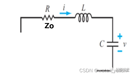
Z = Z 0 + j ( ω L − 1 ω C ) Z=Z_0+j(\omega L-\frac 1 {\omega C}) Z=Z0+j(ωL−ωC1)
Γ = Z − Z 0 Z + Z 0 = j ( ω L − 1 ω C ) 2 Z 0 + j ( ω L − 1 ω C ) = j ( ω L − 1 ω C ) / Z 0 2 + j ( ω L − 1 ω C ) / Z 0 l e t ( ω L − 1 ω C ) / Z 0 = k Γ = j k 2 + j k = k 2 4 + k 2 + j 2 k 4 + k 2 Γ r = k 2 4 + k 2 Γ i = 2 k 4 + k 2 \Gamma=\frac {Z-Z_0} {Z+Z_0}=\frac {j(\omega L-\frac 1 {\omega C})} {2Z_0+j(\omega L-\frac 1 {\omega C})}=\frac {j(\omega L-\frac 1 {\omega C})/Z_0} {2+j(\omega L-\frac 1 {\omega C})/Z_0} \\ let \quad (\omega L-\frac 1 {\omega C})/Z_0=k \\ \Gamma=\frac {jk} {2+jk}=\frac {k^2}{4+k^2}+j\frac {2k}{4+k^2} \\ \Gamma_r=\frac {k^2}{4+k^2} \quad \Gamma_i=\frac{2k}{4+k^2} Γ=Z+Z0Z−Z0=2Z0+j(ωL−ωC1)j(ωL−ωC1)=2+j(ωL−ωC1)/Z0j(ωL−ωC1)/Z0let(ωL−ωC1)/Z0=kΓ=2+jkjk=4+k2k2+j4+k22kΓr=4+k2k2Γi=4+k22k

along the circle r = 1 r=1 r=1, 在谐振的情况下电路实现阻抗匹配。 -
Z L = 2 Z 0 Z_L=2Z_0 ZL=2Z0 with harmonic frequency

Z = 1 + Γ 1 − Γ Z=\frac {1+\Gamma} {1-\Gamma} Z=1−Γ1+Γ Γ = 1 3 e − j 2 β l \Gamma=\frac 13e^{-j2\beta l} Γ=31e−j2βl
| f f f | 0 | f 1 f_1 f1 | f 2 = 2 f 1 f_2=2f_1 f2=2f1 | f 3 = 3 f 1 f_3=3f_1 f3=3f1 | f 4 = 4 f 1 f_4=4f_1 f4=4f1 |
|---|---|---|---|---|---|
| λ \lambda λ | ∞ \infin ∞ | 8 l 8l 8l | 8 l / 2 8l/2 8l/2 | 8 l / 3 8l/3 8l/3 | 8 l / 4 8l/4 8l/4 |
| ∠ Γ \angle\Gamma ∠Γ | 0 | − π / 2 -\pi/2 −π/2 | − π -\pi −π | − 3 π / 2 -3\pi/2 −3π/2 | − 2 π -2\pi −2π |
| ∣ Γ ∣ |\Gamma| ∣Γ∣ | 1/3 | 1/3 | 1/3 | 1/3 | 1/3 |

along the circle
r
=
1
/
3
r=1/3
r=1/3, 达到谐振频率时的点即为圆与垂直/水平轴的交点。
-
Open Transmission Line

Z = − j Z 0 cot β l Z=-jZ_0 \cot\beta l Z=−jZ0cotβl reactance only , Γ = e − j 2 β l \Gamma=e^{-j2\beta l} Γ=e−j2βl

along circle r = 0 r=0 r=0, start from Γ r = 1 \Gamma_r=1 Γr=1, 由图可知,当达到两倍 f 1 f1 f1, 等效于短路 -
Short Transmission Line
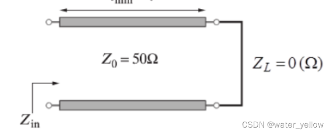
Z = − j Z 0 tan β l Z=-jZ_0 \tan\beta l Z=−jZ0tanβl reactance only , Γ = − e − j 2 β l \Gamma=-e^{-j2\beta l} Γ=−e−j2βl

along circle r = 0 r=0 r=0, start from Γ r = − 1 \Gamma_r=-1 Γr=−1, 和open Transmission Line的情况类似,起点不同,随着频率增大,电路先出现感性电抗(上半圆),后出现容性电抗(下半圆) -
TL terminated with Capacitor
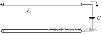
Z = Z 0 1 + Γ 1 − Γ Z=Z_0\frac {1+\Gamma} {1-\Gamma} Z=Z01−Γ1+Γ \,\,\,\,\,\,\,\,\,\,\,\,\,\, Γ = e − j ( θ + 2 β l ) \Gamma=e^{-j(\theta+2\beta l)} Γ=e−j(θ+2βl)

纯电感电路的Smith Chart都是沿着 r = 0 r=0 r=0的最外圆,区别在于起点的不同. 随着频率( β l \beta l βl)增加, 轨迹都是沿着clockwise的方向. -
TL terminated with Inductor
Z = Z 0 1 + Γ 1 − Γ Z=Z_0\frac {1+\Gamma} {1-\Gamma} Z=Z01−Γ1+Γ \,\,\,\,\,\,\,\,\,\,\,\,\,\, Γ = − e − j ( θ + 2 β l ) \Gamma=-e^{-j(\theta+2\beta l)} Γ=−e−j(θ+2βl)
轨迹图和情况8 TL terminated with Indccutor 中的相同
Sample 03 史密斯图求驻波比和回波损耗
For a 50 Ω 50\Omega 50ΩTL with load Z L Z_L ZL,find Γ \Gamma Γ, the SWR(circles), and determine the RL(dB): (a) Z L = 75 + j 25 Z_L=75+j25 ZL=75+j25 (b) Z L = 10 − j 5 Z_L=10-j5 ZL=10−j5 ( c) Z L = 48.5 Z_L=48.5 ZL=48.5
解:
Normalized
(a)
Z
L
=
1.5
+
j
0.5
Z_L=1.5+j0.5
ZL=1.5+j0.5
(b)
Z
L
=
0.2
−
j
0.1
Z_L=0.2-j0.1
ZL=0.2−j0.1
(c )
Z
L
=
0.97
Z_L=0.97
ZL=0.97
在圆上找到
Z
L
Z_L
ZL对应的点, 以圆心(原点)到该点的距离为半径画圆, 该圆与实轴
Γ
r
\Gamma_r
Γr的右交点即为SWR
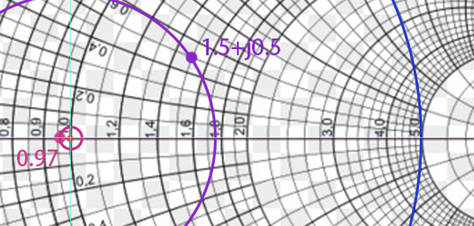
如图,紫色圈是(a), 蓝圈代表(b), magenta色代表(c ), 右交点坐标分别为1.77, 5.0, 1.03 即为对应的SWR.
完整史密斯图的下方有几条刻度尺,其中一条代表Return Loss
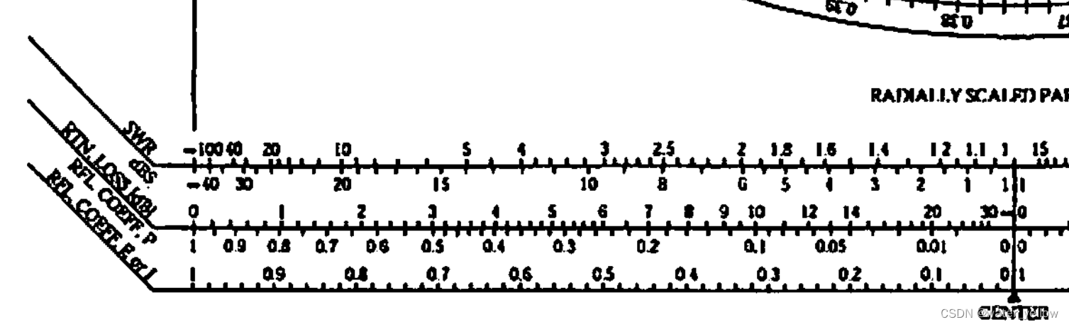
已知Impedance,画出圆以后,做圆的垂直切线,切线与Return Loss轴的交点即为该Impedance对应的RL
其实就是找对应半径的刻度:placing radius of
∣
Γ
∣
|\Gamma|
∣Γ∣ circle on horizontal “RTN Loss (dB)”
三条cyan颜色的垂线与RTN LOSS刻度尺的交点读数分别为:
(a)(中间)
R
L
=
11.3
d
B
RL=11.3 dB
RL=11.3dB
(b)(最左)
R
L
=
3.4
d
B
RL=3.4 dB
RL=3.4dB
(c)(最右)
R
L
>
30
d
B
RL>30 dB
RL>30dB
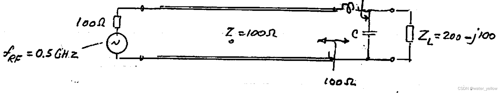
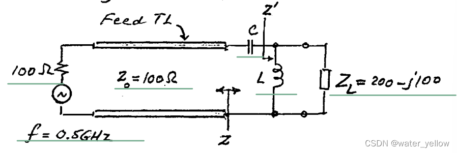
sample 04&05 阻抗匹配的史密斯图表示
Graphical solutions for finding the lumped matching network
Design an L-C matching network for a capacitive load
Z
L
=
200
−
j
100
Ω
Z_L=200-j100\Omega
ZL=200−j100Ω to be matched at
f
R
F
=
0.5
G
H
z
f_{RF}=0.5GHz
fRF=0.5GHz to a
100
Ω
100\Omega
100Ω source and a TL with
Z
0
=
100
Ω
Z_0=100\Omega
Z0=100Ω
解:
1)Normalized:
Z
L
=
200
−
j
100
100
=
2
−
j
Z_L=\frac {200-j100} {100}=2-j
ZL=100200−j100=2−j
2)Find
Y
L
Y_L
YL,
Y
L
Y_L
YL对应点和
Z
L
Z_L
ZL关于原点对称
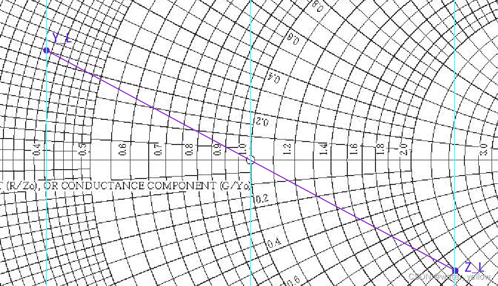
由图,
Y
L
=
0.4
+
j
0.2
Y_L=0.4+j0.2
YL=0.4+j0.2
(3) Adding a shunt capacitive susceptance (+jb)of C should result in a complex impedance
Z
′
Z'
Z′ with
R
e
(
Z
′
)
=
1
Re(Z')=1
Re(Z′)=1. 添加电容C(与
R
L
R_L
RL平行),使得等效阻抗 (记为
Z
′
Z'
Z′) 的实部为1. Matching Network意味着
Z
0
=
Z
l
o
a
d
=
100
Ω
Z_0=Z_{load}=100\Omega
Z0=Zload=100Ω, 标准化以后
Z
l
o
a
d
=
1
Z_{load}=1
Zload=1,没有虚部。虚部必须被抵消。The reactive part will have to be “resonated out” by inductor L.
Z
l
o
a
d
=
1
Z_{load}=1
Zload=1 is the original point on Smith Chart.
添加电容后的Admittance记为
Y
′
Y'
Y′ (
Z
′
Z'
Z′ 的相反数)。添加电容后Impedance(Admittance)的实部不变,所以
Y
′
Y'
Y′ 和
Y
L
Y_L
YL在同一个圆上,
R
e
(
Y
L
)
=
R
e
(
Y
′
)
=
0.4
Re(Y_L)=Re(Y')=0.4
Re(YL)=Re(Y′)=0.4.
Z
′
Z'
Z′ 和
Y
′
Y'
Y′关于原点对称,
Z
′
Z'
Z′ 在
r
=
1
r=1
r=1的圆上,在史密斯图上画出这两点:

读数:
Y
′
≈
0.4
+
j
0.48
Z
′
=
1
−
j
1.23
Y'\approx0.4+j0.48\,\,\,\,\,\,Z'=1-j1.23
Y′≈0.4+j0.48Z′=1−j1.23
C(susceptance of C)在图上表示为:沿着圆r=0.4(clockwise),由
Y
L
Y_L
YL 到
Y
′
Y'
Y′的弧线
L( reactance of L)在图上表示为:沿着圆r=1(clockwise), 由
Z
′
Z'
Z′到
Z
l
o
a
d
Z_{load}
Zload(即原点)的弧线,即resonated out the reactance.

j
0.48
−
j
0.2
=
j
0.28
j0.48-j0.2=j0.28
j0.48−j0.2=j0.28, susceptance of C after denormalize:
B
=
2.8
×
1
0
−
3
B=2.8\times10^{-3}
B=2.8×10⁻³
C
=
B
2
π
f
R
F
=
0.89
p
F
C=\frac B {2\pi f_{RF}}=0.89pF
C=2πfRFB=0.89pF
reactance of L after denormalize:
X
=
23
X=23
X=23,
L
=
X
2
π
f
R
F
=
39.2
n
H
L=\frac X {2\pi f_{RF}}=39.2nH
L=2πfRFX=39.2nH
Design the C-L matching network in the circuit below to match a load
Z
L
=
300
−
j
100
Ω
Z_L=300-j100\Omega
ZL=300−j100Ω to a signal source with impedance of
100
Ω
100\Omega
100Ω, which is itself matched to a feed TL (
Z
0
=
100
Ω
Z_0=100\Omega
Z0=100Ω). The operating frequency is
f
=
0.5
G
H
z
f=0.5GHz
f=0.5GHz
解:
(1)Normalize:
Z
L
=
2
−
j
Z_L=2-j
ZL=2−j, find
Z
L
Z_L
ZL on smith Chart, and fine
Y
L
=
0.4
+
j
0.2
Y_L=0.4+j0.2
YL=0.4+j0.2
(2) 并联电感L 以后,ademittance实部不变,虚部沿着逆时针方向增加,
Y
′
Y'
Y′仍在圆
r
=
0.4
r=0.4
r=0.4 上,对应的
Z
′
Z'
Z′实部为1,在圆
r
=
1
r=1
r=1上,
Y
′
&
Z
′
Y' \& Z'
Y′&Z′ 关于原点对称,找出这两点。
Y
′
=
0.4
−
j
0.5
Y'=0.4-j0.5
Y′=0.4−j0.5,
Z
′
=
1
+
j
1.2
Z'=1+j1.2
Z′=1+j1.2

(3)
Y
′
−
Y
L
=
j
0.7
=
n
o
r
m
a
l
i
z
e
d
s
u
s
c
e
p
t
a
n
c
e
o
f
i
n
d
u
c
t
o
r
L
Y'-Y_L=j0.7=normalized \,susceptance \,of\, inductor\, L
Y′−YL=j0.7=normalizedsusceptanceofinductorL
L
=
1
B
∗
2
π
f
R
F
=
45.47
n
H
L=\frac 1{B*2\pi f_{RF}}=45.47nH
L=B∗2πfRF1=45.47nH
为了保证
Z
l
o
a
d
Z_{load}
Zload虚部为0,加上电容C resonance out the reactance, 从
Z
′
Z'
Z′沿着
r
=
1
r=1
r=1逆时针方向回到原点的弧线段表示C
normalized reactance of C=
1.2
j
1.2j
1.2j
C
=
1
X
∗
2
π
f
R
F
=
2.65
p
F
C=\frac 1{X*2\pi f_{RF}}=2.65pF
C=X∗2πfRF1=2.65pF

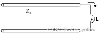
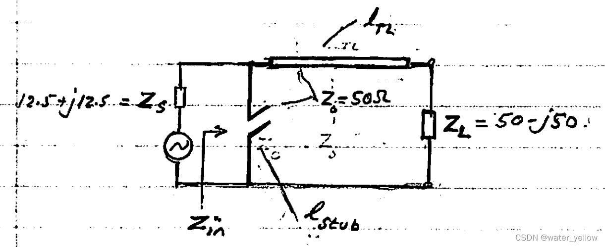
Sample 06 确定传输线和Stub的长度
Transmission Line and Stub Match
Design the stub-TL Z-matching network below to match a source
Z
S
=
12.5
+
j
12.5
Ω
Z_S=12.5+j12.5\Omega
ZS=12.5+j12.5Ω to a load
Z
L
=
50
−
j
50
Ω
Z_L=50-j50\Omega
ZL=50−j50Ω.
Z
0
=
50
Ω
Z_0=50\Omega
Z0=50Ω(for the TL and stub.) the objective is M.P.T(
Z
i
n
=
Z
s
∗
Z_{in}=Z_s^*
Zin=Zs∗). Find the length of TL and Stub
解:
(1)normalize(
Z
/
Z
0
Z/Z_0
Z/Z0):
Z
S
=
0.25
+
j
0.25
Z
L
=
1
−
j
Z_S=0.25+j0.25\,\,\,\,\,\,\,\,\,\,Z_L=1-j
ZS=0.25+j0.25ZL=1−j
(2)Find the conjugate of
Z
S
Z_S
ZS- same real part and inversed imaginary part,so the conjugate point and the original
Z
S
Z_S
ZS is symmetric about real axis
Z
S
∗
=
0.25
−
j
0.25
Z_S^*=0.25-j0.25
ZS∗=0.25−j0.25
(3)Conver Z to Y, find
Y
S
∗
Y^*_S
YS∗ and
Y
L
Y_L
YL
Show on the Smith Chart

Y
S
∗
=
2.1
+
j
2.0
Y^*_S=2.1+j2.0
YS∗=2.1+j2.0
Y
L
=
0.5
+
j
0.5
Y_L=0.5+j0.5
YL=0.5+j0.5
(4)draw
Γ
\Gamma
Γ circle for
Y
L
Y_L
YL, 就是以圆心到
Y
L
Y_L
YL的距离为半径画圆
(5)rotate
Y
L
Y_L
YL along that circle toward generator until intersection with conductance circle of
Y
S
∗
Y^*_S
YS∗, intersection point is
A
A
A。
A
A
A点是画出的圆和
Y
S
∗
Y^*_S
YS∗ 所在的圆(
r
=
2.1
r=2.1
r=2.1)的交点。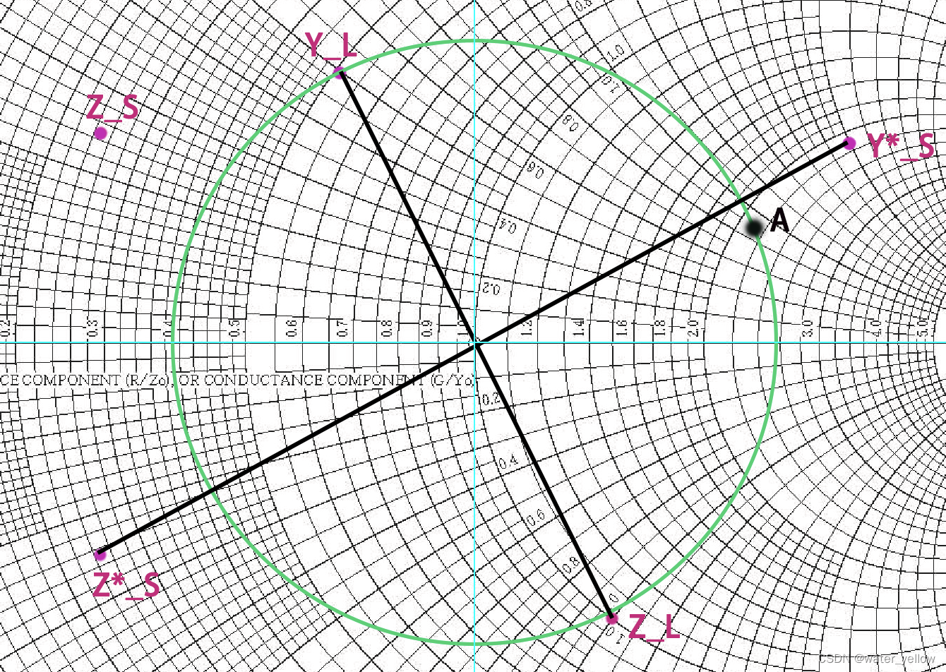
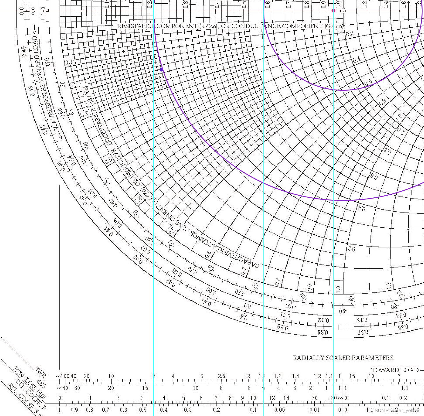
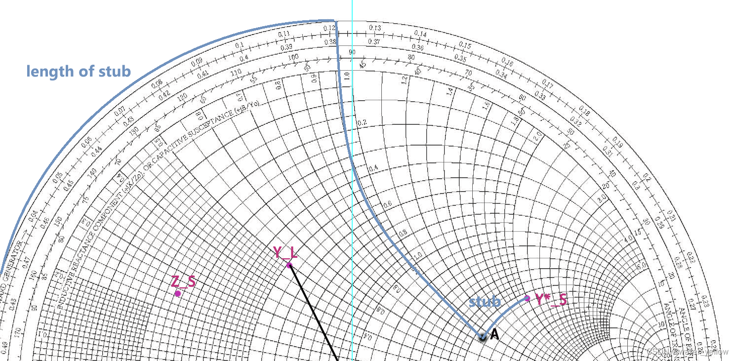
(6)从最外圈“length toward generator”找到
A
A
A和
Y
L
Y_L
YL对应的点,方法是连接圆心和该点,延长这条直线,找到与外圈刻度尺的交点。两个刻度之差就是TL的长度(注意是相对于波长
λ
\lambda
λ而言),大约是
0.212
−
0.087
=
0.125
λ
0.212-0.087=0.125\lambda
0.212−0.087=0.125λ

(7)
A
=
2.1
+
j
1.1
A=2.1+j1.1
A=2.1+j1.1 和
Y
S
∗
=
2.1
+
j
2
Y^*_S=2.1+j2
YS∗=2.1+j2 之间的弧长(沿着conductance circle r=2.1)即对应susceptance(admittance)of stub=
j
1.1
j1.1
j1.1,
y
s
t
u
b
=
0.9
j
y_{stub}=0.9j
ystub=0.9j. Find the length of stub from the outside circle, moving from
y
=
0
y=0
y=0 (open term) to
j
1.1
j1.1
j1.1(在外圈找到
X
=
j
1.1
X=j1.1
X=j1.1对应的length,就是大约虚轴的位置), aprroximate
0.122
λ
0.122\lambda
0.122λ
(8)second solution. Notice that the green circle in step (6) has the other intersection point with addmitance circle
r
=
2.1
r=2.1
r=2.1, marked as B, so length from
Y
L
Y_L
YL to B coule be the orther length of TL, length from B to
y
∗
s
y*_s
y∗s coule be the orther susceptance of stub
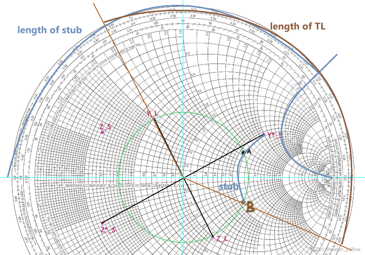
B
=
2.1
−
j
1.1
B=2.1-j1.1
B=2.1−j1.1, normalized susceptance of stub=
j
2
−
(
−
j
1.1
)
=
j
3.1
j2-(-j1.1)=j3.1
j2−(−j1.1)=j3.1, 图中的蓝线标出了
j
3.1
j3.1
j3.1对应的"length toward genertator", from
y
=
0
y=0
y=0 to
y
=
3.1
y=3.1
y=3.1(外圈的蓝色长弧线), the aprroximate length of stub is
0.198
λ
0.198\lambda
0.198λ, 棕色的弧线是length of TL,大约是"
0.288
−
0.088
=
0.2
λ
0.288-0.088=0.2\lambda
0.288−0.088=0.2λ"
Sample 07 史密斯图与放大器的稳定性
Instability:
∣
Γ
∣
2
>
1
|\Gamma|^2 >1
∣Γ∣2>1, reflected > incidented
Stability:
∣
Γ
∣
2
<
1
|\Gamma|^2 <1
∣Γ∣2<1
Define the output stability circle with
{
C
e
n
t
e
r
:
C
L
=
S
22
∗
−
S
11
Δ
∗
∣
S
22
2
∣
−
∣
Δ
∣
2
R
a
d
i
u
s
:
R
L
=
∣
S
12
S
21
∣
S
22
2
∣
−
∣
Δ
∣
2
∣
\begin{cases} Center: & C_L=\frac {S_{22}^* -S_{11}\Delta^*} {|S_{22}^2 |- |\Delta|^2}\\ Radius: & R_L=|\frac {S_{12}S_{21}} {|S_{22}^2 |- |\Delta|^2}| \end{cases}
{Center:Radius:CL=∣S222∣−∣Δ∣2S22∗−S11Δ∗RL=∣∣S222∣−∣Δ∣2S12S21∣
represent it on the
Γ
L
\Gamma_L
ΓL axis:
∣
Γ
L
−
C
L
∣
2
=
R
L
2
|\Gamma_L-C_L|^2=R_L^2
∣ΓL−CL∣2=RL2
2 Cases:
∣
S
11
<
1
∣
|S_{11}<1|
∣S11<1∣ &
∣
S
11
>
1
∣
|S_{11}>1|
∣S11>1∣
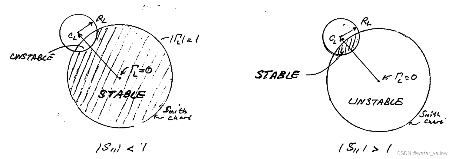
(1)
∣
S
11
<
1
∣
|S_{11}<1|
∣S11<1∣ . For
Γ
L
=
0
\Gamma_L=0
ΓL=0,
∣
Γ
i
n
∣
=
∣
S
11
+
S
12
S
21
Γ
L
1
−
S
22
Γ
L
∣
=
∣
S
11
∣
<
1
|\Gamma_{in}|=|S_{11}+\frac {S_{12}S_{21}\Gamma_L}{1-S_{22}\Gamma_L}|=|S_{11}|<1
∣Γin∣=∣S11+1−S22ΓLS12S21ΓL∣=∣S11∣<1, POINT
Γ
L
\Gamma_L
ΓL belongs to stable region, whitch is outside the stability circle. Thus, the stable region is that outside the stability circle falling with in the Smith Chart.
(2) ∣ S 11 > 1 ∣ |S_{11}>1| ∣S11>1∣ . For Γ L = 0 \Gamma_L=0 ΓL=0, ∣ Γ i n ∣ = ∣ S 11 + S 12 S 21 Γ L 1 − S 22 Γ L ∣ = ∣ S 11 ∣ > 1 |\Gamma_{in}|=|S_{11}+\frac {S_{12}S_{21}\Gamma_L}{1-S_{22}\Gamma_L}|=|S_{11}|>1 ∣Γin∣=∣S11+1−S22ΓLS12S21ΓL∣=∣S11∣>1, POINT Γ L \Gamma_L ΓL belongs to unstable region, whitch is outside the stability circle. Thus, the stable region is that inside the stability circle falling with in the Smith Chart.
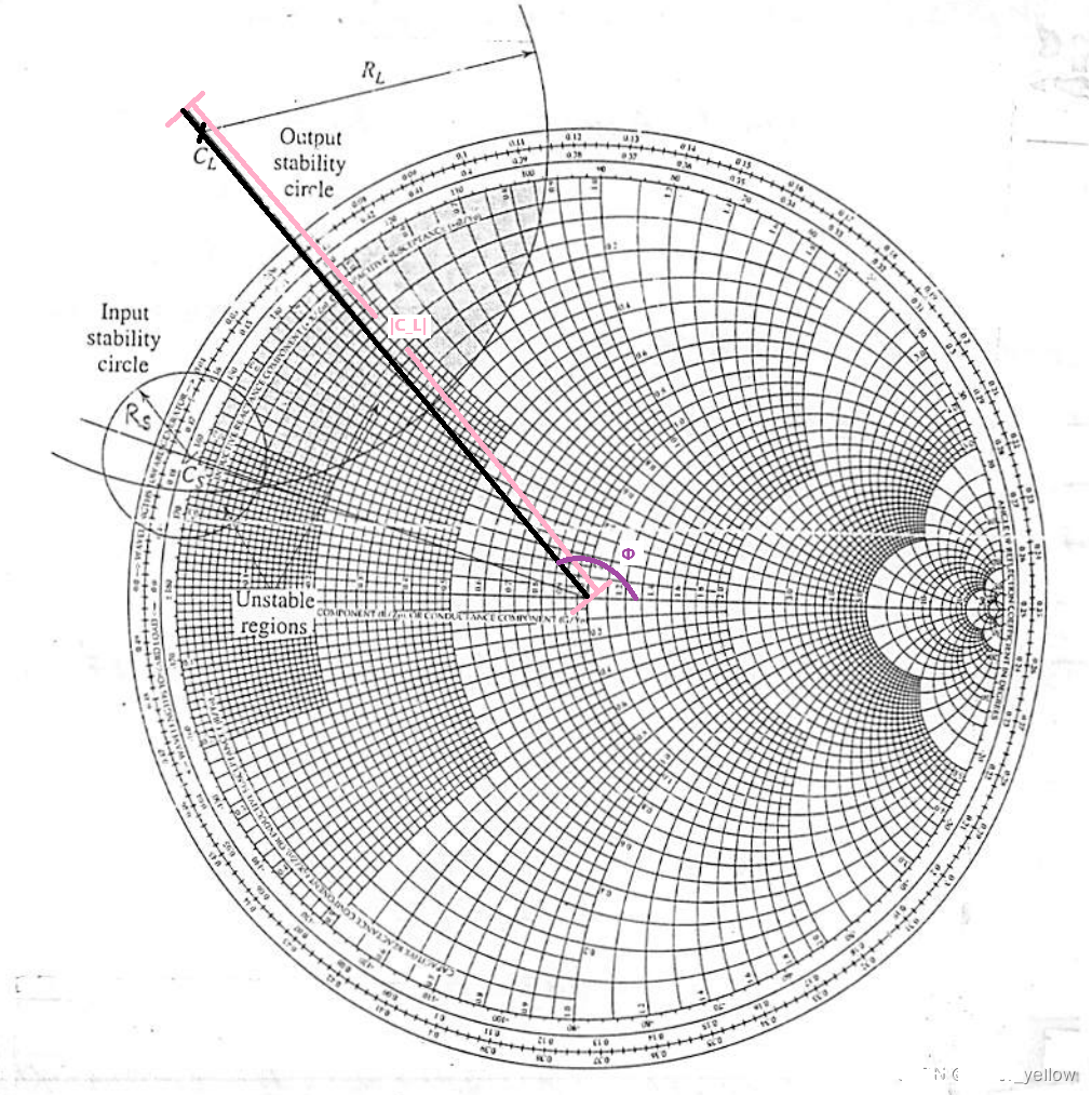
How to plot stability circle(以output circle 为例子)
(1)使用上述公式求出
C
L
=
∣
C
L
∣
∠
ϕ
C_L=|C_L|\angle \phi
CL=∣CL∣∠ϕ和
R
L
R_L
RL
(2)在史密斯图上确定圆心和半径
Tips
- The Smith Chart is a graphical mapping of Γ \Gamma Γ into Z Z Z(must be normalized)
- 最大的圆代表 r = 0 r=0 r=0,其与“x轴/水平轴”的左交点为代表短路,右交点代表开路,圆心代表阻抗匹配。
- 上半平面的点对应
R
L
RL
RL,reactance
x
>
0
x>0
x>0
下半平面的点对应 R C RC RC,reactance x < 0 x<0 x<0
先写到这里。这个图的用处和学问还有很多,但短时间内没办法研究透彻,仅将目前所学内容复盘呈上,如能有所帮助,不胜荣幸。
![]()


 2771
2771


 被折叠的 条评论
为什么被折叠?
被折叠的 条评论
为什么被折叠?
 到【灌水乐园】发言


