


 本文介绍了一种使用VHDL实现的乘法器设计方法,并详细阐述了其端口定义、IP核生成过程及代码实现细节。通过仿真验证了设计的正确性。
一、 Multiplier
1.1 概述
乘法器顾名思义,用来做乘法运算。
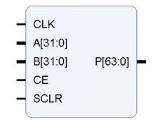
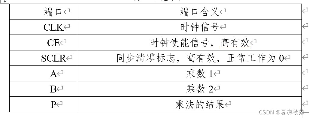
1.2 端口说明
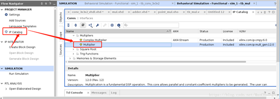
1.3 ip核的生成
(1)在ip catalog里面选择multiplier
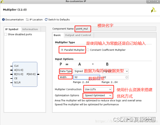
(2)basic的具体配置以及含义如下:
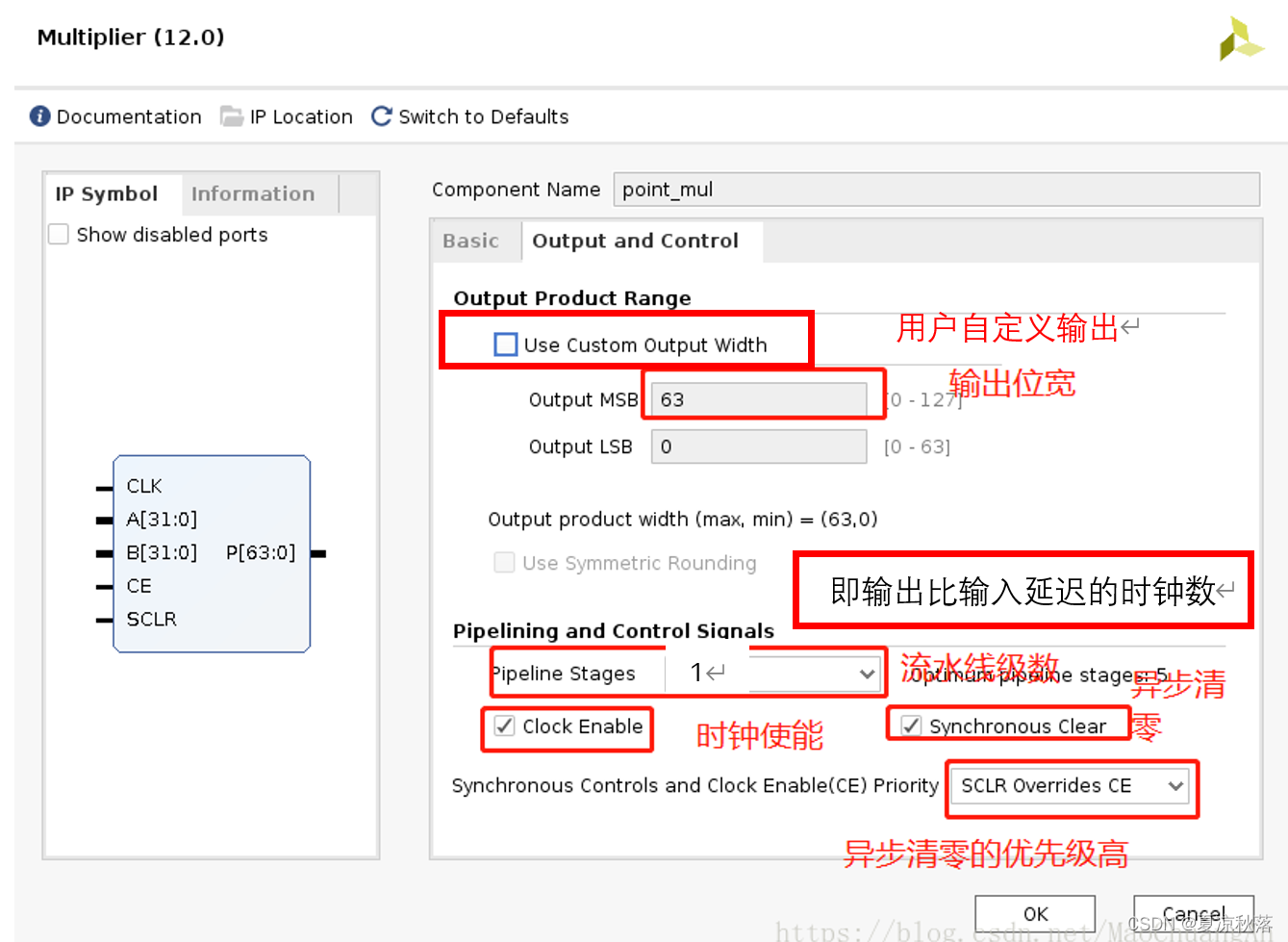
(3)output and control的配置如下:
1.4 代码实现
主程序:
library IEEE;
use IEEE.STD_LOGIC_1164.ALL;

-- Uncomment the following library declaration if using
-- arithmetic functions with Signed or Unsigned values
--use IEEE.NUMERIC_STD.ALL;

-- Uncomment the following library declaration if instantiating
-- any Xilinx leaf cells in this code.
--library UNISIM;
--use UNISIM.VComponents.all;

entity Multiplier is
 Port (
	CLK: in std_logic;
	A : IN STD_LOGIC_VECTOR(31 DOWNTO 0);
  B : IN STD_LOGIC_VECTOR(31 DOWNTO 0);
  CE : IN STD_LOGIC;
  SCLR : IN STD_LOGIC;
  P : OUT STD_LOGIC_VECTOR(63 DOWNTO 0)
	 );
end Multiplier;


architecture Behavioral of Multiplier is
	COMPONENT mult_gen_0
  PORT (
    CLK : IN STD_LOGIC;
    A : IN STD_LOGIC_VECTOR(31 DOWNTO 0);
    B : IN STD_LOGIC_VECTOR(31 DOWNTO 0);
    CE : IN STD_LOGIC;
    SCLR : IN STD_LOGIC;
    P : OUT STD_LOGIC_VECTOR(63 DOWNTO 0)
  );
END COMPONENT;

begin
signed32_signed32 : mult_gen_0
  PORT MAP (
    CLK => CLK,
    A => A,
    B => B,
    CE => CE,
    SCLR => SCLR,
    P => P
  );

end Behavioral;
测试文件(VHDL):
library IEEE;
use IEEE.STD_LOGIC_1164.ALL;
use IEEE.STD_LOGIC_ARITH.ALL;

-- Uncomment the following library declaration if using
-- arithmetic functions with Signed or Unsigned values
--use IEEE.NUMERIC_STD.ALL;

-- Uncomment the following library declaration if instantiating
-- any Xilinx leaf cells in this code.
--library UNISIM;
--use UNISIM.VComponents.all;

entity multiplier_tb is
--  Port ( );
end multiplier_tb;

architecture Behavioral of multiplier_tb is

	signal clk     :    std_logic;
 	signal a       :     std_logic_vector(31 downto 0);
 	signal b       :     std_logic_vector(31 downto 0);
 	signal cs      :     std_logic;
 	signal sclr    :  std_logic;
 	signal result  : std_logic_vector(63 downto 0);

	COMPONENT multiplier
	  Port (
	  CLK: in std_logic;
	  A : IN STD_LOGIC_VECTOR(31 DOWNTO 0);
    B : IN STD_LOGIC_VECTOR(31 DOWNTO 0);
    CE : IN STD_LOGIC;
    SCLR : IN STD_LOGIC;
    P : OUT STD_LOGIC_VECTOR(63 DOWNTO 0)
	  );
 	END COMPONENT;


begin

	 multiplier_inst0: multiplier
	  Port map (
	  CLK  => clk,
	  A    => a,
    B    => b,
    CE   => cs,
    SCLR => sclr,
    P    => result
	  );


	clk_gen: process
	begin
		clk <='1';
		wait for 5ns;
		clk <= '0';
		wait for 5ns;
  end process;

  process
  begin
  	a    <= (others=>'0') ;  -- 必须加括号否则会报错
  	b    <= (others=>'0');
  	cs   <= '0';
  	sclr <='1';
  	wait for 20ns;
  	a    <= conv_std_logic_vector(11,32);
  	b    <= conv_std_logic_vector(10,32);
  	cs   <= '1';
  	sclr <='0';
    wait for 100ns;
    a    <= conv_std_logic_vector(-11,32);
  	b    <= conv_std_logic_vector(10,32);
  	wait for 100ns;
    cs <='0';
    wait;   -- 一直等待下去

 end process;


end Behavioral;
测试文件(Verilog):
module multiplier_tb1();

reg clk;
reg signed [31:0] a;
reg signed [31:0] b;
reg cs;
reg sclr;
wire signed [63:0] result ;

 Multiplier Multiplier_inst0
  (
	.CLK   (clk),
	.A     (a),
  .B     (b ),
  .CE    (cs ),
  .SCLR  (sclr ),
  .P     (result)
	 );

initial clk=1;
always #5 clk=~clk;

initial begin
	  a    = 0 ;
  	b    = 0;
  	cs   = 0;
  	sclr =1;
    #20;
  	a    = 32'd11;
  	b    = 32'd10;
  	cs   = 1;
  	sclr = 0;
    #100;
    a    = $signed(-11);
  	b    = 32'd10;
  	#100;
    cs =0;
end


endmodule
1.5 仿真结果
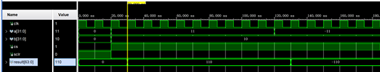
从图中可以看出,输出比输入延时了一个时钟周期,这与ip核中pipeline stages设置一样,而且乘法运算结果正确。


 1221
1221

 被折叠的 条评论
为什么被折叠?
被折叠的 条评论
为什么被折叠?
 到【灌水乐园】发言


