


AN9238模块数据采集
1 AN9238原理
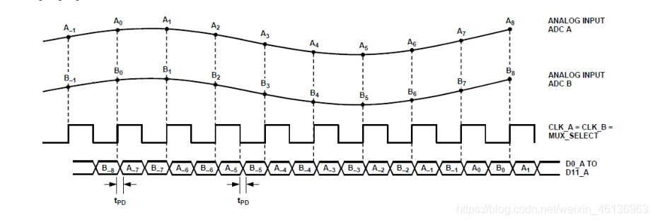
根据时序图,只要FPGA输出两路时钟信号作为AD模块的AD_clk,便可以采集数据。
其他原理见数据手册
2 板上验证
顶层模块
`timescale 1ns / 1ps
module top(
input clk50m, //系统时钟
input reset_n,
output wire [0:0] clk65m_1, //FPGA输出的时钟信号1,作为AD模块的输入时钟1
output wire [0:0] clk70m_1, //FPGA输出的时钟信号2,作为AD模块的输入时钟2
input wire [11:0] ad1_in, // 离散数据输入到FPGA
input wire [11:0] ad2_in
);
/****************PLL 产生65M时钟和50M时钟 **************/
//首先PLL产生两路时钟clk65m、clk70m;
//然后将这两个时钟赋值给FPGA的输出时钟clk65m_1和clk70m_1;
//ADC时,将clk65m_1和clk70m_1赋值给ADC的时钟
wire clk65m;
wire clk70m;
assign clk65m_1=clk65m;
assign clk70m_1=clk70m;
pll pll_inst
(
// Clock out ports
.clk_out1(clk65m), // output clk_out1
.clk_out2(clk70m), // output clk_out2
// Status and control signals
.reset(~reset_n), // input reset
.locked( ), // output locked
// Clock in ports
.clk_in1(clk50m)
); // input clk_in1
/**************** AD 转化模块 ADC数据采样**************/
wire [11:0] ad_ch1;
wire [11:0] ad_ch2;
v_ad v_ad_inst (
.ad1_clk(clk65m_1) ,//65M
.ad2_clk(clk65m_1) ,//65M
.ad1_in(ad1_in),//模拟数据输入到AD模块
.ad2_in(ad2_in),
.ad_ch1(ad_ch1),AD模块输出数字数据
.ad_ch2(ad_ch2)
);
/**************** fifo**************/
wire wr_en=1; //写使能
wire rd_en=1; //读使能
wire [11:0] dout; // 读数据
wire full; //写满信号
wire empty; //读空信号
wire [9 : 0] rd_data_count ;// 可读数据数量
wire [9 : 0] wr_data_count ;//已写入的数据数量
fifo_generator_1 fifo_wr_inst (
.rst (~reset_n), // input wire rst
.wr_clk (clk65m), // input wire wr_clk
.rd_clk (clk70m), // input wire rd_clk
.din (ad1_in), // input wire [11 : 0] din
.wr_en (wr_en), // input wire wr_en
.rd_en (rd_en), // input wire rd_en
.dout (dout), // output wire [11 : 0] dout
.full (full), // output wire full
.empty (empty), // output wire empty
.rd_data_count(rd_data_count), // output wire [9 : 0] rd_data_count
.wr_data_count(wr_data_count) // output wire [9 : 0] wr_data_count
);
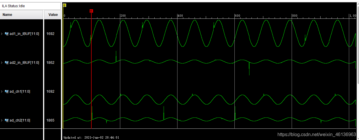
// 例化ila,观察波形
ila_0 ila_0_inst (
.clk(clk50m), // input wire clk
.probe0(ad1_in), // input wire [11:0] probe0 input
.probe1(ad2_in), // input wire [11:0] probe1
.probe2(ad_ch1), // input wire [11:0] probe2 output
.probe3(ad_ch2), // input wire [11:0] probe3
.probe4(ad1_in), // input wire [11:0] probe4
.probe5(dout), // input wire [11:0] probe5
.probe6(rd_data_count), // input wire [9:0] probe6
.probe7(wr_data_count), // input wire [9:0] probe7
.probe8(clk65m), // input wire [0:0] probe8
.probe9(clk70m) // input wire [0:0] probe9
);
endmodule
上面调用了两个三个IP核:
pll:产生65M和70M的时钟信号。
fifo:将AD采集的数据送到fifo中缓存。
ila:观察信号。
AD采集模块
`timescale 1ns / 1ps
// AD 转化模块

module v_ad(
             input              ad1_clk ,//65M
             input              ad2_clk ,//65M
			 input [11:0]       ad1_in  ,
 			 input [11:0]       ad2_in  ,

			 output reg [11:0]  ad_ch1  ,
 			 output reg [11:0]  ad_ch2

    );
//通道1采集数据
always @(posedge ad1_clk)//根据时序,只要给时钟信号clk_A就可以采集数据,在上升沿采集数据
begin
    ad_ch1 <= ad1_in;
end

//通道2采集数据
always @(posedge ad2_clk)//根据时序,只要给时钟信号clk_A就可以采集数据,在上升沿采集数据
begin
    ad_ch2 <= ad2_in;
end

endmodule
约束文件
############## clock and reset define##################
create_clock -period 20.000 [get_ports clk50m]
set_property IOSTANDARD LVCMOS33 [get_ports clk50m]
set_property PACKAGE_PIN U18 [get_ports clk50m]

set_property IOSTANDARD LVCMOS33 [get_ports reset_n]
set_property PACKAGE_PIN N15 [get_ports reset_n]


##############AX7020 and AX7010  J11##################
set_property PACKAGE_PIN F16 [get_ports {ad2_in[0]}]
set_property PACKAGE_PIN F20 [get_ports {ad2_in[1]}]
set_property PACKAGE_PIN F19 [get_ports {ad2_in[2]}]
set_property PACKAGE_PIN G20 [get_ports {ad2_in[3]}]
set_property PACKAGE_PIN G19 [get_ports {ad2_in[4]}]
set_property PACKAGE_PIN H18 [get_ports {ad2_in[5]}]
set_property PACKAGE_PIN J18 [get_ports {ad2_in[6]}]
set_property PACKAGE_PIN L20 [get_ports {ad2_in[7]}]
set_property PACKAGE_PIN L19 [get_ports {ad2_in[8]}]
set_property PACKAGE_PIN M20 [get_ports {ad2_in[9]}]
set_property PACKAGE_PIN M19 [get_ports {ad2_in[10]}]
set_property PACKAGE_PIN K18 [get_ports {ad2_in[11]}]


set_property PACKAGE_PIN H20 [get_ports {ad1_in[1]}]
set_property PACKAGE_PIN J20 [get_ports {ad1_in[0]}]
set_property PACKAGE_PIN L17 [get_ports {ad1_in[3]}]
set_property PACKAGE_PIN L16 [get_ports {ad1_in[2]}]
set_property PACKAGE_PIN M18 [get_ports {ad1_in[5]}]
set_property PACKAGE_PIN M17 [get_ports {ad1_in[4]}]
set_property PACKAGE_PIN D20 [get_ports {ad1_in[7]}]
set_property PACKAGE_PIN D19 [get_ports {ad1_in[6]}]
set_property PACKAGE_PIN E19 [get_ports {ad1_in[9]}]
set_property PACKAGE_PIN E18 [get_ports {ad1_in[8]}]
set_property PACKAGE_PIN G18 [get_ports {ad1_in[11]}]
set_property PACKAGE_PIN G17 [get_ports {ad1_in[10]}]


set_property PACKAGE_PIN H17 [get_ports  clk65m_1]
set_property IOSTANDARD LVCMOS33 [get_ports clk65m_1]
set_property PACKAGE_PIN F17 [get_ports  clk70m_1]
set_property IOSTANDARD LVCMOS33 [get_ports clk70m_1]

set_property IOSTANDARD LVCMOS33 [get_ports {ad1_in[*]}]
set_property IOSTANDARD LVCMOS33 [get_ports {ad2_in[*]}]

#set_property IOB true [get_ports ad2_in[*]]
#set_property IOB true [get_ports ad1_in[*]]

create_debug_core u_ila_0 ila
set_property ALL_PROBE_SAME_MU true [get_debug_cores u_ila_0]
set_property ALL_PROBE_SAME_MU_CNT 1 [get_debug_cores u_ila_0]
set_property C_ADV_TRIGGER false [get_debug_cores u_ila_0]
set_property C_DATA_DEPTH 1024 [get_debug_cores u_ila_0]
set_property C_EN_STRG_QUAL false [get_debug_cores u_ila_0]
set_property C_INPUT_PIPE_STAGES 0 [get_debug_cores u_ila_0]
set_property C_TRIGIN_EN false [get_debug_cores u_ila_0]
set_property C_TRIGOUT_EN false [get_debug_cores u_ila_0]
set_property port_width 1 [get_debug_ports u_ila_0/clk]
connect_debug_port u_ila_0/clk [get_nets [list pll_inst/inst/clk_out1]]
set_property PROBE_TYPE DATA_AND_TRIGGER [get_debug_ports u_ila_0/probe0]
set_property port_width 12 [get_debug_ports u_ila_0/probe0]
connect_debug_port u_ila_0/probe0 [get_nets [list {v_ad_inst/ad1_in[0]} {v_ad_inst/ad1_in[1]} {v_ad_inst/ad1_in[2]} {v_ad_inst/ad1_in[3]} {v_ad_inst/ad1_in[4]} {v_ad_inst/ad1_in[5]} {v_ad_inst/ad1_in[6]} {v_ad_inst/ad1_in[7]} {v_ad_inst/ad1_in[8]} {v_ad_inst/ad1_in[9]} {v_ad_inst/ad1_in[10]} {v_ad_inst/ad1_in[11]}]]
create_debug_port u_ila_0 probe
set_property PROBE_TYPE DATA_AND_TRIGGER [get_debug_ports u_ila_0/probe1]
set_property port_width 12 [get_debug_ports u_ila_0/probe1]
connect_debug_port u_ila_0/probe1 [get_nets [list {v_ad_inst/ad2_in[0]} {v_ad_inst/ad2_in[1]} {v_ad_inst/ad2_in[2]} {v_ad_inst/ad2_in[3]} {v_ad_inst/ad2_in[4]} {v_ad_inst/ad2_in[5]} {v_ad_inst/ad2_in[6]} {v_ad_inst/ad2_in[7]} {v_ad_inst/ad2_in[8]} {v_ad_inst/ad2_in[9]} {v_ad_inst/ad2_in[10]} {v_ad_inst/ad2_in[11]}]]
create_debug_port u_ila_0 probe
set_property PROBE_TYPE DATA_AND_TRIGGER [get_debug_ports u_ila_0/probe2]
set_property port_width 12 [get_debug_ports u_ila_0/probe2]
connect_debug_port u_ila_0/probe2 [get_nets [list {v_ad_inst/ad_ch2[0]} {v_ad_inst/ad_ch2[1]} {v_ad_inst/ad_ch2[2]} {v_ad_inst/ad_ch2[3]} {v_ad_inst/ad_ch2[4]} {v_ad_inst/ad_ch2[5]} {v_ad_inst/ad_ch2[6]} {v_ad_inst/ad_ch2[7]} {v_ad_inst/ad_ch2[8]} {v_ad_inst/ad_ch2[9]} {v_ad_inst/ad_ch2[10]} {v_ad_inst/ad_ch2[11]}]]
create_debug_port u_ila_0 probe
set_property PROBE_TYPE DATA_AND_TRIGGER [get_debug_ports u_ila_0/probe3]
set_property port_width 12 [get_debug_ports u_ila_0/probe3]
connect_debug_port u_ila_0/probe3 [get_nets [list {v_ad_inst/ad_ch1[0]} {v_ad_inst/ad_ch1[1]} {v_ad_inst/ad_ch1[2]} {v_ad_inst/ad_ch1[3]} {v_ad_inst/ad_ch1[4]} {v_ad_inst/ad_ch1[5]} {v_ad_inst/ad_ch1[6]} {v_ad_inst/ad_ch1[7]} {v_ad_inst/ad_ch1[8]} {v_ad_inst/ad_ch1[9]} {v_ad_inst/ad_ch1[10]} {v_ad_inst/ad_ch1[11]}]]
set_property C_CLK_INPUT_FREQ_HZ 300000000 [get_debug_cores dbg_hub]
set_property C_ENABLE_CLK_DIVIDER false [get_debug_cores dbg_hub]
set_property C_USER_SCAN_CHAIN 1 [get_debug_cores dbg_hub]
connect_debug_port dbg_hub/clk [get_nets clk50m_IBUF]
结果分析
3 仿真
仿真文件
`timescale 1ns / 1ps

module sim_top;

    //input
    reg clk50m;
    reg reset_n;
    reg [11:0] ad1_in;
    reg [11:0] ad2_in;

    //output
    wire [11:0] ad_ch1;
    wire [11:0] ad_ch2;
    // 初始化
    top top_inst(
    //input
        .clk50m(clk50m),
        .reset_n(reset_n),
        .ad1_in(ad1_in),
        .ad2_in(ad2_in)

//         //output  对于FPGA来说,是输入
//         .ad_ch1(ad_ch1),
//         .ad_ch2(ad_ch2)

        );

 //--------------模拟产生顶层模块所需的输入信号
//1、模拟产生时钟信号和复位信号
    initial
    begin
     //初始化输入
        clk50m=0;
        reset_n=0;
        #1000;
        reset_n=1;
    end
    // create clock;
    always #10 clk50m=~clk50m;


 //2模拟产生两个通道待采集的模拟数据
 always @(posedge clk50m or negedge reset_n )
 begin
     if (reset_n==1'b0)
            begin
               ad1_in <=12'd0;
               ad2_in <=12'd0;
            end
     else
            begin
                   ad1_in <=ad1_in+1'd1;
                   ad2_in <=ad2_in+2'd2;
            end
end

endmodule
仿真结果
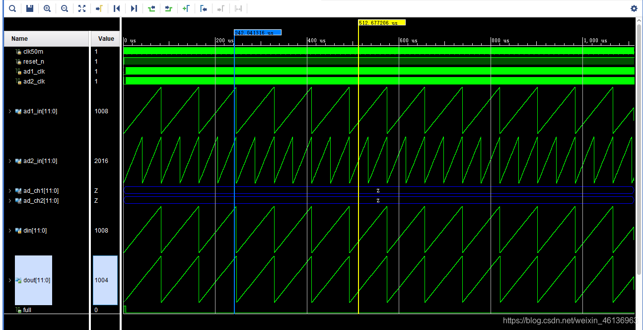


 3795
3795

 被折叠的 条评论
为什么被折叠?
被折叠的 条评论
为什么被折叠?
 到【灌水乐园】发言


