


视频链接
PCIe转SATA电路设计
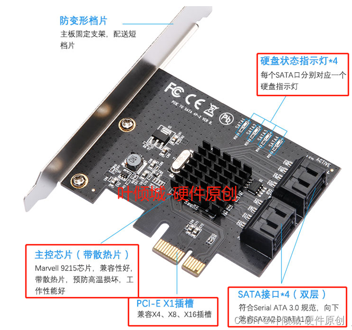
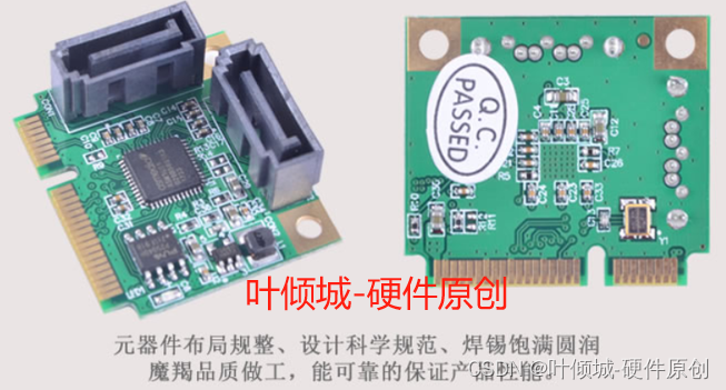
1、PCIe转SATA电路设计基本介绍
2、PCIe转SATA的两种方案(京东)
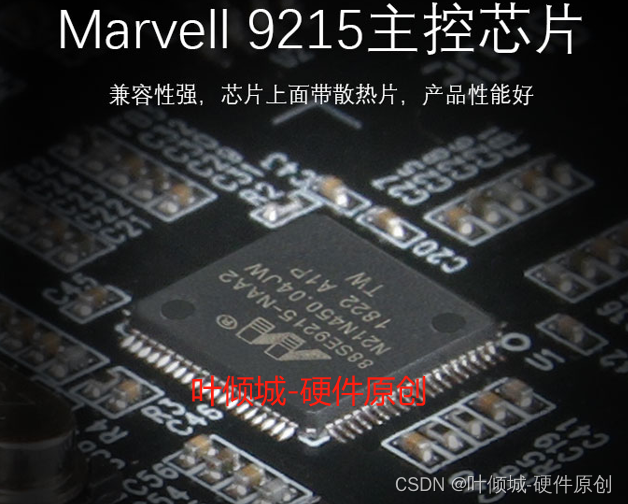
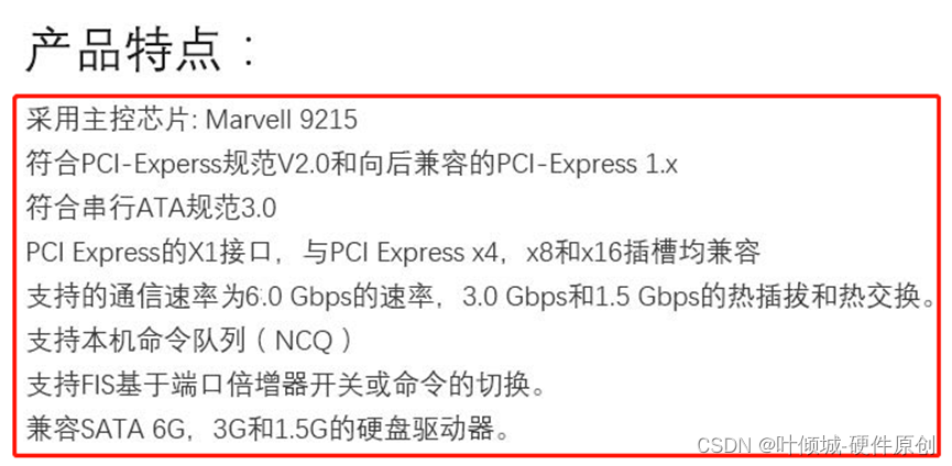
2.1、Marevell(美满)88SE9215
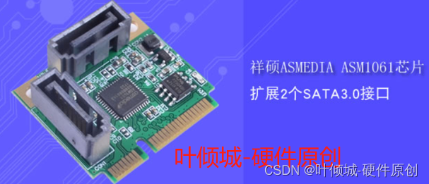
2.2、ASMEDIA(祥硕)ASM1061
3、套片、桥片、PCIE switch等基本介绍
3.1、套片(不需要)
3.2、PCIE switch
PCIe Switch高级功能及应用

3.3、桥片
3.4、CPU本身自带的PCIE接口
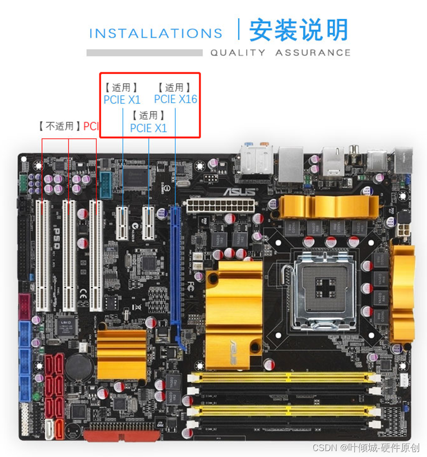
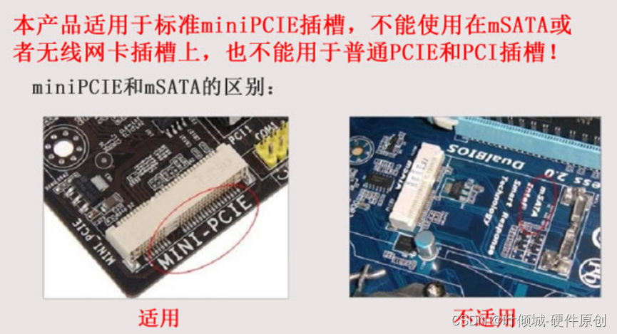
4、以超威主板为例

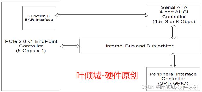
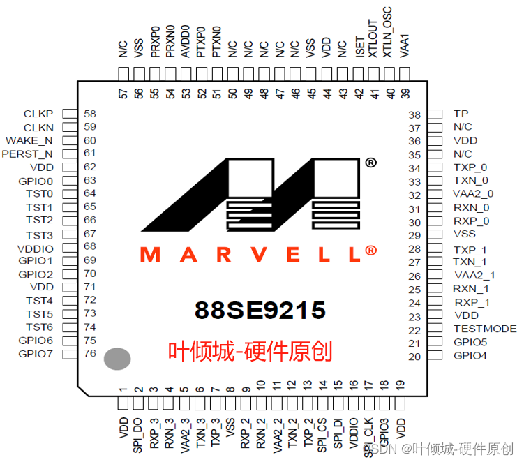
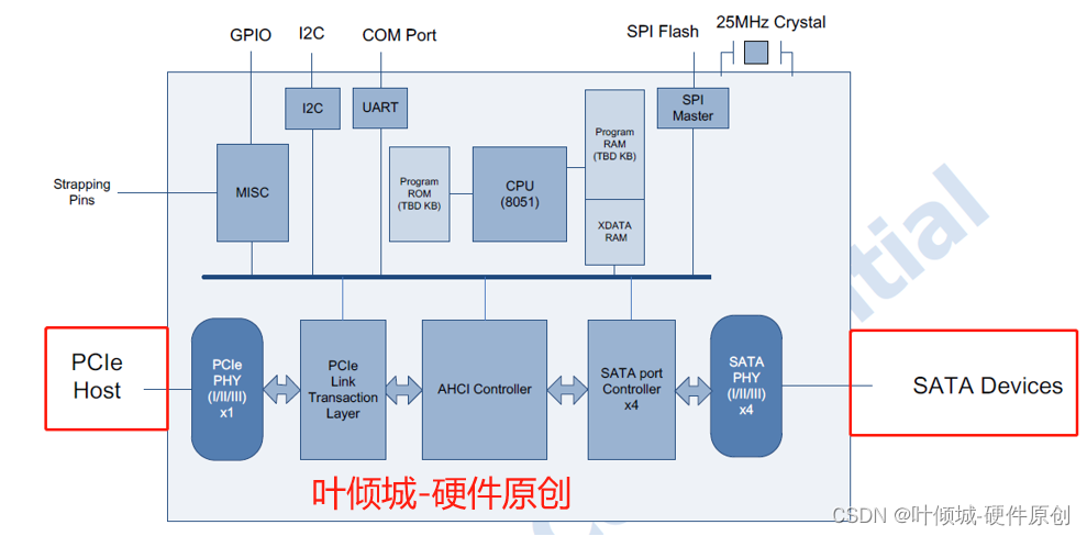
5、PCIe转SATA(以88SE9215为例)
5.1、结构框图
88SE9125和88SE9215两者的区别在于
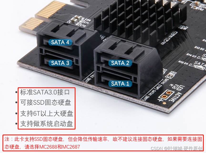
88SE9215 转出4路SATA
88SE9125 转出2路SATA
55 nm CMOS process, 1.0V digital core, 1.8V analog, and 3.3V I/O power supplies.
Reference clock frequency of 25 MHz, provided by an external clock source or generated by an external crystal oscillator.
5.2、信号定义
5.2.1、Power supply
对于电源电压,系统要求
| 管脚符号 | 类型 | 描述 |
| VAA2_0 VAA2_1 VAA2_2 VAA2_3 | Analog Power | 1.8V analog power supply for SATA PHY. |
| VAA1 | Analog Power | 1.8V analog power for crystal oscillator, reference current generator, and PLL. |
| AVDD0 | Analog Power | 1.8V analog power supply for PCIe PHY |
| VDDIO | I/O Power | 3.3V analog power supply for digital I/Os |
| VDD | Power | 1.0V Core Digital Power. |
| VSS | GND | Ground.The main ground is the exposed die-pad (ePad) on the bottom side of the package. |
5.2.2、PCIe Interface Signals
| 管脚符号 | 类型 | 描述 |
| PERST_N | I, PU | PCI Platform Reset.Active low。 |
| WAKE_N | O, OD | PCI Wake-Up. An open-drain, active low signal that is driven low by a PCIe function to reactivate the PCIe Link hierarchy’s main power rails and reference clocks. |
| CLKP CLKN | I/A | Reference Clock. Low voltage differential signals. The clock frequency has to be 100 MHz. |
| PRXP0 PRXN0 | I/A | PCIe differential signals to the controller’s receiver. |
| PTXP0 PTXN0 | O/A | PCIe differential signals from the controller’s transmitter. |
5.2.3、Serial ATA Interface Signals
4组SATA。4收4发,实际是16根线!
| 管脚符号 | 类型 | 描述 |
| TXN_[0:3] TXP_[0:3] | O/A | Serial ATA Transmitter Differential Outputs. |
| RXN_[0:3] RXP_[0:3] | I/A | Serial ATA Receiver Differential Inputs. |
5.2.4、Reference Signals
| 管脚符号 | 类型 | 描述 |
| ISET | I/O A | Reference Current for Crystal Oscillator and PLL.This pin has to be connected to an external 6.04 kΩ 1% resistor to Ground. 晶体振荡器和锁相环的参考电流。这个引脚必须连接到一个外部的6.04 kΩ 1%电阻到地。 |
| XTLOUT | O/ A | Crystal Output. |
| XTLIN_OSC | I/ A | Reference Clock Input. This signal can be from an oscillator, or connected to a crystal with the XTLOUT pin. The clock frequency must be 25 MHz ± 80 ppm. |
5.2.5、General Purpose I/O Signals
| 管脚符号 | 类型 | 描述 |
| GPIO[0:7] | I/O, PU | General Purpose I/O. |
5.2.6、SPI Flash Interface Signals
| 管脚符号 | 类型 | 描述 |
| SPI_CLK | O | SPI Interface Clock. |
| SPI_DI | I, PU | Serial Data In. Connect to the serial flash device’s serial data output (DO). |
| SPI_CS | O | SPI Interface Chip Select. |
| SPI_DO | O | Serial Data Out.Connect to the serial flash device’s serial data input (DI). |
5.2.7、Test Mode Interface Signals
| 管脚符号 | 类型 | 描述 |
| TP | I/O, A | Analog Test Point for PCIe PHY, SATA PHY, crystal oscillator,and PLL. |
| TST[0:6] | I/O | Test Pin.This pin is reserved for chip test purposes only. Keep floating. |
| TESTMODE | I, PD | Test Mode.Enables chip test modes. |
5.2.8、No Connect Signals
| 管脚符号 | 类型 | 描述 |
| NC | N/A | No Connect |
集合:76pin
| Pin Description | 数目(个) |
| Power & Gnd | 19 |
| PCIe Interface Signals | 8 |
| Serial ATA Interface Signals | 16 |
| Reference Signals | 3 |
| General Purpose I/O Signals | 8 |
| SPI Flash Interface Signals | 4 |
| Test Mode Interface Signals | 9 |
| No Connect Signals | 9 |
6、PCIe转SATA(以ASM1064为例)
6.1、结构框图


 447
447

 被折叠的 条评论
为什么被折叠?
被折叠的 条评论
为什么被折叠?
 到【灌水乐园】发言


